Search icon CANCEL
Subscription
0
Cart icon
Your Cart (0 item)
Close icon
You have no products in your basket yet
Arrow left icon
Explore Products
Best Sellers
New Releases
Books
Videos
Audiobooks
Learning Hub
Free Learning
Arrow right icon
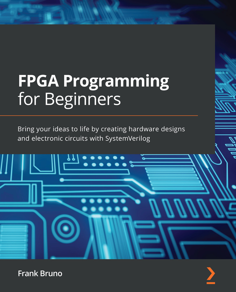
FPGA Programming for Beginners

FPGA Programming for Beginners: Bring your ideas to life by creating hardware designs and electronic circuits with SystemVerilog

eBook
€24.99 €35.99
Paperback
€44.99
Subscription
Free Trial
Renews at €18.99p/m

What do you get with Print?

Product feature icon Instant access to your digital eBook copy whilst your Print order is Shipped
Product feature icon Paperback book shipped to your preferred address
Product feature icon Download this book in EPUB and PDF formats
Product feature icon Access this title in our online reader with advanced features
Product feature icon DRM FREE - Read whenever, wherever and however you want
Product feature icon AI Assistant (beta) to help accelerate your learning
OR
Modal Close icon
Payment Processing...
tick Completed

Shipping Address

Billing Address

Shipping Methods
Table of content icon View table of contents Preview book icon Preview Book

FPGA Programming for Beginners

Chapter 1: Introduction to FPGA Architectures and Xilinx Vivado

In the following chapter, we will be exploring Field Programmable Gate Arrays (FPGAs) and the underlying technology that creates them. This underlying technology allows companies such as Xilinx to produce a reprogrammable chip from an Application Specific Integrated Circuit (ASIC) process. We'll then learn how to use an FPGA for a simple task. Whether you want to accelerate mathematically complex operations such as machine learning or artificial intelligence, or simply want to do some projects for fun, such as retro computing or reproducing obsolete video game machines (https://github.com/MiSTer-devel/Main_MiSTer/wiki), this book will jumpstart your journey. There couldn't be a better time to get into this field than the present, even if only as a hobby. Development boards are cheap and plentiful, and vendors have started making their tools available for free for their low cost, smaller parts.

In this book, we are going to build some example designs to introduce you to FPGA development, culminating in a project that can drive a VGA monitor.

By the end of this chapter, you should have a good understanding of an FPGA and its components.

In this chapter, we are going to cover the following main topics:

  • What is an ASIC?
  • How does a company create an FPGA?
  • What makes up an FPGA?
  • How can we use the Xilinx Vivado tools to design, test, and implement an FPGA

Technical requirements

To follow along with the examples in this chapter, you need the following hardware and software.:

Hardware

Unlike programming languages, SystemVerilog is a hardware description language, and to really see the fruits of your work in this book, you will need an FPGA board to load your designs into. For the purposes of this book, I am suggesting one of two development boards, which are readily available. It is possible to target another board if you already have one. However, some of the resources may not be identical or you may need to change the constraints file (xdc) to access the resources that another board has:

The Nexys A7 is preferable if possible because it has external interfaces that will be discussed in later chapters and will give you experience interfacing to external components. I would recommend the 100T in case you get ambitious and would like to explore more as the price difference is relatively small and it has twice the resources. With the exception of the DDR memory, the Basys 3 board can do most of the projects, although some may require the purchase of PMOD interface boards.

Software

You need the following software to follow along:

What is an ASIC?

ASICs are the fundamental building blocks of modern electronics – your laptop or PC, TV, cell phone, digital watch, almost everything you use on a day-to-day basis. It is also the fundamental building block upon which the FPGA we will be looking at is built from. In short, an ASIC is a custom-built chip designed using the same language and methods we will be introducing in this book.

FPGAs came about as the technology to create ASICs followed Moore's law (Gordon E. Moore, Cramming more components onto integrated circuits, Electronics, Volume 38, Number 8 (https://newsroom.intel.com/wp-content/uploads/sites/11/2018/05/moores-law-electronics.pdf) – the idea that the number of transistors on a chip doubles every 2 years. This has allowed for both very cheap electronics in the case of mass-produced items containing ASICs and led to the proliferation of lower cost FPGAs.

Why an ASIC or FPGA?

ASICs can be an inexpensive part when manufactured in high volumes. You can buy a disposable calculator, a flash drive for pennies per gigabyte, an inexpensive cell phone; they are all powered by at least one ASIC. ASICs are also sometimes a necessity when speed is of the utmost importance, or the amount of logic that is needed is very large. However, in these cases, they are typically only used when cost is not a factor.

We can break down the costs of developing a product based on an ASIC or FPGA into Non-Recurring Engineering (NRE), the one-time cost to develop a chip, and the piece price for every chip, excluding NRE. Ed Sperling states the following in CEO Outlook: It Gets Much Harder From Here, Semiconductor Engineering, June 3, 2019, https://semiengineering.com/ceo-outlook-the-easy-stuff-is-over/:

"The NRE for a 7nm chip is $25 million to $30 million, including mask set and labor."

These costs include more than just the mask sets, the blueprint for the ASIC if you will, that is used to deposit the materials on the silicon wafers that build the chip. It's also the teams of design, implementation, and verification engineers that can number into the hundreds. Usually factored into ASIC costs are re-spins, which are bug fixes. These are a factor because large, complex devices struggle with first-time success.

Compare this to an FPGA. Fairly complex chips can be developed by a single person, or small teams. Most of the NRE has been shouldered by the FPGA vendor in the design of the FPGA chips, which are known good quantities. What little NRE is left is for tools and engineering. Re-spins are free, except for time, since the chip can be reprogrammed without million-dollar mask sets.

The trade-off is the per part cost. High volume ASICs with low complexity, like the one inside a pocket calculator or a digital watch, can cost pennies. CPUs can run into the hundreds or thousands of dollars. FPGAs, even the most inexpensive Spartan-7, start at a few dollars and the largest and fastest can stretch into the tens of thousands of dollars.

Another factor is tool costs. As we will see later in this chapter, Xilinx provides the Vivado tool suite for free in the form of a webpack for the smaller parts. This speeds adoption, where the barrier to entry is now a computer and a development board. Even the cost of developing more expensive parts is only a few thousand dollars if you need to purchase a professional copy of Vivado. ASIC tools can run into the millions of dollars and require years of training since the risk of failure is so high. As we will see in our projects, we'll make mistakes, sometimes to demonstrate a concept, but the cost to fix it will only be a few minutes of time, mostly to understand why it failed:

Figure 1.1 – Simple ASIC versus FPGA flow

Figure 1.1 – Simple ASIC versus FPGA flow

The flow for an ASIC or FPGA is essentially the same. ASIC flows tend to be more linear, in that you have one chance to make a working part. With an FPGA, things such as simulation can become an option, although strongly suggested for complex designs. One difference is that the lab debug stage can also act as a form of simulation by using ChipScope, or similar on-chip debugging techniques, to monitor internal signals for debugging. The main difference is that each iteration through the steps costs only time in an FPGA flow. In this situation, any changes to a fabricated ASIC design requires some number of new mask sets that can run into the millions of dollars.

We've briefly looked at what an ASIC is and why we might choose an ASIC or an FPGA for a given application. Now, let's take a look at how an FPGA is created using an ASIC process.

How does a company create a programmable device using an ASIC process?

The basis of any ASIC technology is the transistor, with the largest devices holding up to a billion. There are multiple ASIC processes that have been developed over the years, and they all rely on 0s and 1s, in other words, on or off transistors. These on or off transistors can be thought of as Booleans, true or false values.

The basis of Boolean algebra was developed by George Bool in 1847. The fundamentals of Boolean algebra make up the basis of the logic gates upon which all digital logic is formed. The code that we will be writing will be at a fairly high level, but it is important to understand the basics and it will give us a good springboard for a first project.

Fundamental logic gates

There are four basic logic gates. We typically write the truth tables for the gates to understand their functionality. A truth table shows us what the output is for every set of inputs to a circuit. Refer to the following example involving a NOT gate.

Important note

In this section, we are primarily discussing only the logical functions. There are equivalent bitwise functions that will be introduced. Logical functions are typically used in if statements, bitwise functions in logic operations.

Assign statement

In SystemVerilog, we can use an assign statement to take whatever value is on the right-hand side of the equal sign to the left-hand side. Its usage is as follows:

assign out = in; 

in can be another signal, function, or operation on multiple signals. out can be any valid signal declared prior to the assign statement.

Comments

SystemVerilog provides two ways of commenting. The first is using a double slash, //. This type of comment runs until the end of the line it's located on. The second type of comment is a block comment. Both are shown here:

// Everything here is a comment./* I can span    Multiple    Lines */

if statement

SystemVerilog provides a way of testing conditions via the if statement. The basic syntax is as follows:

if (condition) event

We will discuss if statements in more detail in Chapter 2, Combinational Logic.

Logical NOT (!)

The output of the NOT gate produces the inverse of the signal going in. The function in SystemVerilog can be written as follows:

assign out = !in; // logical or boolean operator

The associated truth table is as follows:

Figure 1.2 – NOT gate representation

Figure 1.2 – NOT gate representation

The NOT gate is one of the most common operators we will be using:

if (!empty) ...

Often, we need to test a signal before performing an operation. For example, if we are using a First in First Out (FIFO) storage to smooth out sporadic data or for crossing clock domains, we'll need to test whether there is data available before popping it out for use. FIFOs have flags used for flow control, the two most common being full and empty. We can do this by testing the empty flag, as shown previously.

We will go into greater depth in later chapters on how to design a FIFO as well as use one.

Logical AND (&&), bitwise AND (&)

Often, we will want to test whether one or more conditions are active at the same time. To do this, we will be using the AND gate.

The function in SystemVerilog can be written as follows:

assign out = in1 && in0; // logical or boolean operator

The associated truth table is as follows:

Figure 1.3 – AND gate representation

Figure 1.3 – AND gate representation

Continuing our FIFO example, you might be popping from one FIFO and pushing into another:

if (!src_fifo_empty && !dst_fifo_full) ...

In this case, you want to make sure that both the source FIFO has data (is not empty) and that the destination is not full. We can accomplish this by testing it via the if statement.

Logical OR (||), bitwise OR (|)

Another common occurrence is to check whether any one signal out of a group is set to perform an operation.

The function in SystemVerilog can be written as follows:

assign out = in1 || and in0; // logical or boolean operator

The associated truth table is as follows:

Figure 1.4 – OR gate representation

Figure 1.4 – OR gate representation

Next, we will look at the exclusive OR function.

XOR (^)

The exclusive OR function checks whether either one of two inputs is set, but not both. The function in SystemVerilog can be written as follows:

assign out = in1 ^ and in0; // logical or boolean operator

The associated truth table is as follows:

Figure 1.5 – XOR gate representation

Figure 1.5 – XOR gate representation

This function is used in building adders, parity, and error correcting and checking codes. In the next section, we'll look at how an adder is built using the preceding gates.

More complex operations

We've looked at the basic components in the previous sections that make up every digital design. Here we'll look at an example of how we can put together multiple logic gates to perform work. For this we will introduce the concept of a full adder. A full adder takes three inputs, A, B, and carry in, and produces two outputs, sum and carry out. Let's look at the truth table:

Figure 1.6 – Full adder

Figure 1.6 – Full adder

The SystemVerilog code for the full adder written as Boolean logic would be as follows:

assign Sum = A ^ B ^ Cin;
assign Cout = A & B | (A^B) & Cin;

You'll notice that we are using the bitwise operators for AND (&) and OR (|) since we are operating on bits. From this straightforward, yet important example, you can see that real-world functionality can be built from these basic building blocks. In fact, all the circuits in an ASIC or FPGA are built this way, but luckily you don't need to dive into this level of detail unless you really want to thanks to the proliferation of High-Level Design Languages (HDLs), such as SystemVerilog.

Introducing FPGAs

A gate array in ASIC terms is a sea of gates with some number of mask steps that can be configured for a given application. This allows for a more inexpensive product since the company designing the ASIC only needs to pay for the masks necessary for configuring. The FPGA takes this one step further by providing the programmability of the fabric as part of the device. This does result in an increased cost as you are paying for interconnect you are not using and the storage devices necessary to configure the FPGA fabric, but allows for some cost reductions as these parts become standard devices that can be mass produced.

If we look at the functions in the previous section through the adder example, we can see one commonality; they can all be produced using a truth table. This becomes key in FPGA development. We can regard these truth tables as Read Only Memory (ROM) representations of the functions. In fact, we can regard them as Programmable ROMs (PROMs) in the case of building up our FPGA.

Let's take the example of the fundamental logic functions. We can reproduce any of them by utilizing a 2-input lookup table, which could look something like this:

Figure 1.7 – Two input LUT examples

Figure 1.7 – Two input LUT examples

This is an oversimplified example, but what we have are four storage elements, in this case flip-flops, but in the case of an actual FPGA, more likely a much simpler structure utilizing far fewer transistors. The storage elements are connected to one another such that their configuration can be loaded. By attaching other Lookup Tables (LUTs) to the chain, multiple LUTs can be configured at startup, or in the case of partial reconfiguration, during normal operation. By adding a flip-flop, we can see the final structure of the LUT take shape.

The power in the simplicity of the structure is the ability to replicate this design many times over. In the case of modern FPGAs, they are built of many tiles or columns of logic such as this, allowing a much simpler piece to be designed, implemented, and verified, and then replicated to produce the large gate count devices available. This allows for a range of lower cost devices with fewer columns of resources to larger devices with many more, some even using Stacked Silicon Interconnects (SSI), which allows multiple ASIC dies to be attached together via an interconnect substrate.

In 1985, Xilinx introduced the XC2064, what we would consider the first FPGA utilizing an array of 64 3-input LUTs with one flip-flop. The breakthrough with this design was that it was modular and had good interconnect resources. This entire part would be approximately equivalent to 1 Combination Logic Block (CLB) in the Artix-7 we will be targeting.

At the heart of an FPGA is the programmable fabric. The fabric consists of LUTs with associated flip-flops making up slices and ultimately CLBs. These blocks are all connected using a rich topology of routing channels, allowing for almost limitless configuration. FPGAs also contain many other resources that we will explore over the course of this book, block RAMs, Serial-Deserial (SERDES) cores, DSP elements, and many types of programmable I/O.

Exploring the Xilinx Artix-7 and 7 series devices

The FPGAs we will be looking at in this book are the Artix-7 series of devices. These devices are the highest performance per watt of the Xilinx 7 series devices. For a reasonable price, they feature a large amount of relatively high-performance logic to implement your designs. The FPGA components we will introduce here are common in the Spartan (low end), Kintex (mid-range) and Virtex (high end) parts in the 7 series.

Combinational logic blocks

ASICs are made up of logic gates based upon libraries provided by ASIC foundries, such as TSMC or Tower. These libraries can contain everything from AND, OR, and NOT gates to more complicated math cells and storage elements. When developing an FPGA, you will be targeting the same Boolean logic equations as you would in an ASIC. We will be using a very similar flow. However, the synthesis process will target the CLBs of the FPGA:

Figure 1.8 – Xilinx UG474 7 series FPGAs CLB users' guide figure 1-1 (used with permission)

Figure 1.8 – Xilinx UG474 7 series FPGAs CLB users' guide figure 1-1 (used with permission)

A CLB consists of a pair of slices, each of which contains four 6-input LUTs and their eight flip-flops. Vivado (or optionally a third-party synthesis tool such as Synopsys Synplify) compiles the SystemVerilog code and maps it to these CLB elements. To fully explore the details of the CLB, I would suggest reading Xilinx UG474, 7 Series FPGAs CLB users' guide (https://www.xilinx.com/support/documentation/user_guides/ug474_7Series_CLB.pdf). At a high level, each LUT allows a degree of flexibility such that any Boolean function with 6 inputs can be implemented or two arbitrarily defined 5-input functions if they share common inputs. There is also dedicated high speed carry logic for arithmetic functions, which will be discussed in later chapters.

The slices come in two formats, SLICEL (logic) and SLICEM (memory). SLICEM is a superset of SLICEL. SLICEM adds the ability to configure the SLICE into a distributed RAM or shift register. There are approximately three times the number of SLICELs as SLICEMs. The following table for the two suggested development boards for this book shows the breakdown:

Although it is theoretically possible to instantiate and force the functionality of lower-level components, such as slices or LUTs, this is beyond the scope of this book, and a feature not widely used. We will be targeting CLB usage through Vivado synthesis of the HDL that we write.

Storage

Aside from the SLICEMs that make up the CLBs that can be used as memories or shift registers, FPGAs contain Block RAMs (BRAM) that are larger storage elements. The 7 series parts all have 36 Kb BRAM that can be split into two 18 Kb BRAMs. The following table shows the BRAM available in the parts on the recommended development boards:

BRAMs can be configured as follows:

  • True dual port memories – Two read/write ports.
  • Simple dual port memories – 1 read/1 write. In this case, a 36 Kb BRAM can be up to 72 bits wide and an 18 Kb BRAM up to 36 bits wide.
  • A single port.

Contents of BRAMs can be loaded at initialization and configured via a file or initial block in the code. This can be useful for implementing ROMs or start up conditions.

BRAMs in 7 series devices also contain logic to implement FIFOs. This saves CLB resources and reduces synthesis overhead and potential timing problems in a design. We will go over FIFOs in a later chapter.

All 36 Kb BRAMs have dedicated Error Correction Code (ECC) functions. As this is something more related to high reliability applications, such as medical-, automotive-, or space-based, something we will not go into detail on in this book.

Clocking

7 series devices implement a rich clocking methodology, which can be explored in detail in UG472 7 Series FPGAs clocking resources user guide (https://www.xilinx.com/support/documentation/user_guides/ug472_7Series_Clocking.pdf). For most purposes, our discussion in the PLL section will give you everything you need to know; however, the referenced document will delve into far more detail.

I/Os

For the most part, we will limit ourselves to the I/Os supported by the two targeted development boards. In general, the 7 series devices handle a variety of interfaces from 3.3v CMOS/TTL to LVDS and memory interface types. The boards we are using will dictate the I/Os defined in our project files. For more information on all the supported types, you can reference the UG471 7 Series FPGAs SelectIO resources user guide.

DSP48E1

FPGAs have a large footprint in Digital Signal Processing (DSP) applications that use a lot of multipliers and, more specifically, Multiply Accumulate (MAC) functions. One of the first innovations in FPGAs was to include hard multipliers followed by DSP blocks that could implement MAC functions:

Figure 1.9 – Xilinx UG479 7 series DSP48E1 users' guide figure 1-1 (used with permission)

Figure 1.9 – Xilinx UG479 7 series DSP48E1 users' guide figure 1-1 (used with permission)

One of the most expensive operations in an FPGA is arithmetic. In an ASIC, the largest and slowest operation is typically a multiplication operation, and the smaller or faster operation is an add operation. For this reason, for many years, FPGA manufacturers have been implementing hard arithmetic cores in their fabric. This makes the opposite true in an FPGA, where the slower operation is typically an adder, especially as the widths get larger. The reason for this is that the multiply has been hardened into a complex, pipelined operation. We will explore the DSP operator more in later chapters. The UG479 7 Series DSP48E1 user guide (https://www.xilinx.com/support/documentation/user_guides/ug479_7Series_DSP48E1.pdf) is a good reference if you are interested in delving into the details.

ASMBL architecture

The 7 series devices are the fourth generation where Xilinx has used the Advanced Silicon Modular Block (ASMBL) architecture for implementation purposes. The idea behind this is to enable FPGA platforms optimized for different target applications. Looking at the 7 series families, we can see how different configurations of slices are brought together to achieve these goals. We can see how the pieces we covered in this chapter are arranged as columns to give us the resources we will be using for our example projects ahead:

Figure 1.10 – Xilinx UG474 7 series FPGAs CLB users' guide figure 2-1 (used with permission)

Figure 1.10 – Xilinx UG474 7 series FPGAs CLB users' guide figure 2-1 (used with permission)

Now that we have looked at what makes up the Artix-7 and other 7 series, we need to get the Xilinx tools installed so that we can get to our first project.

Introduction to the Vivado toolset and evaluation boards

In this section, we will explore the evaluation boards recommended for the projects in this book. We will walk through a very simple design using Vivado to introduce the tool and show how to program the board and demonstrate the functionality of the FPGA.

Evaluation boards

There is no shortage of FPGA evaluation boards available for us to purchase. One company that makes very affordable boards is Digilent. There are several nice features that their boards tend to include, but one of the best is that they have a USB to UART controller built in that Xilinx Vivado recognizes as a programming cable. This makes configuring the device painless. The recommended boards also have the added advantage of being powered over this same USB cable.

Nexys A7 100T (or 50T)

The Nexys A7 is the recommended board for this book. It has all the devices we'll target over the course of the book:

Figure 1.11 – Digilent Nexys A7 board

Figure 1.11 – Digilent Nexys A7 board

The board features are as follows:

  • Artix-7 XC7A100T or 50T
  • 450+MHz operation
  • 128 MB DDR2
  • Serial Flash
  • Built-in USB UART for downloading images and ChipScope debugging
  • MicroSD card reader
  • 10/100 Ethernet PHY
  • PWM audio output/microphone input
  • Temperature sensor
  • 3 axis accelerometer
  • 16 switches
  • 16 LEDs
  • 5 pushbuttons
  • Two 3 color LED
  • Two 4-digit 7-segment displays
  • USB host device support
  • Five PMOD (one XADC)

Let's take a look at the breakdown of the two devices the Nexys board can be ordered with:

One benefit to choosing the XC7A100T is the additional RAM. Especially when starting out you may find yourself relying on chip debugging using ChipScope and the additional RAM will allow for additional storage for wider busses or longer capture times. We'll discuss ChipScope in a later chapter.

Basys 3

An alternative evaluation board is the Basys 3:

Figure 1.12 – Digilent Basys 3 board

Figure 1.12 – Digilent Basys 3 board

This board has the same pushbuttons, LEDs, and switches, but only half the number of seven segment displays. We'll be developing code that can run on either board using these features. It does lack the DDR2 RAM, so it will limit using this for a framebuffer as we will introduce in a later chapter. It is also missing the temperature sensor, microphone, and audio, which we'll look at regarding serial interfaces. PMOD boards can be purchased that have this functionality, however, to overcome this limitation.

The board features are as follows:

  • Artix-7 XC7A35T
  • 450+Mhz operation
  • 128MB DDR2
  • Serial Flash
  • Built-in USB UART for downloading images and ChipScope debugging
  • MicroSD card reader
  • 10/100 Ethernet PHY
  • PWM audio output/microphone input
  • 16 switches
  • 16 LEDs
  • 5 pushbuttons
  • Two 3-color LEDs
  • Single 4-digit, 7-segment displays
  • USB host device support
  • Four PMODs (one dual purpose supporting XADC)

Let's now take a look at the breakdown of the Basys 3 board:

Important note

The Basys 3 board lacks the DDR 2 memory, accelerometers, and audio capabilities, which will be addressed in later chapters. PMODs are available for everything apart from the DDR2. I would recommend the Nexys A7 over the Basys if possible.

We've just taken a look at the boards we are planning on using for the book. Now we need to take a look at the Xilinx tool, Vivado, which will be what we use to design, simulate, implement, and debug our FPGA designs.

Introducing Vivado

Once you have selected a board, the best way to get to know it is to work through an example design.

Vivado is the Xilinx tool we will be using to implement, test, download, and debug our designs. It can be run as a command-line tool in non-project mode, or in project mode using the GUI. For our purposes, we will be using project mode via the GUI; however, we will go through non-project mode as an introduction in the Appendix.

Vivado installation

Xilinx makes Vivado freely available in the form of a webpack for smaller devices. The webpack contains all the features of the full version with a limitation based on device support. It is available for either Windows or Linux. This book will show screenshots for the Linux version; however, everything is tested on both, so you will be fine with using either.

Important note

The Xilinx webpack forces tool feedback information to Xilinx. The paid version allows this to be disabled.

Perform the following steps to effect installation:

  1. Create an account at https://www.xilinx.com/.
  2. Visit https://www.xilinx.com/support/download.html.
  3. Download the Xilinx Unified Installer. For this book, we'll be using version 2020.1.
  4. On Windows, run the .exe file.

    On Linux, use the following commands:

    chmod +x Xilinx_Unified_2020.1_0602_1208_Lin64.bin; ./Xilinx_Unified_2020.1_0602_1208_Lin64.bin
  5. Enter your account information for the installation.
  6. When prompted, you can install either Vitis or Vivado. We will not be using Vitis, but it includes Vivado, so if you are adventurous and want to try Vitis out, feel free to install this as well.
  7. When prompted for the devices, you only need the 7 Series.
  8. Pick an installation location or use the default option.

Once you've completed these steps, get a cup of coffee… take a nap… write a book. It is going to take a while.

Directory structure

With Vivado installed, we can now walk through a very simple project to introduce you to Vivado and to make sure everything is set up correctly. The directory structure I like to use looks like the following:

Figure 1.13 – Directory structure

Figure 1.13 – Directory structure

Items in bold are directories. For our first example design, we do not have a lot of code. We will end up creating only three files: the HDL source code, the testbench, and a constraints file.

Inside the hdl directory, we'll create a simple design, logic_ex.sv, to run through Vivado:

Logic_ex.sv

`timescale 1ns/10ps
module logic_ex
  (
   input  wire  [1:0]    SW,
   output logic [3:0]    LED
   );
  assign LED[0]  = !SW[0];
  assign LED[1]  = SW[1] && SW[0];
  assign LED[2]  = SW[1] || SW[0];
  assign LED[3]  = SW[1] ^ SW[0];
  endmodule // logic_ex

First, we'll define the timescale that we will be operating at in the simulator. 1ns/10ps was pretty standard years ago and for what we'll be doing, it will work fine. If you get involved using high-speed transceivers, you may encounter even smaller timescales, such as 1ps/1fs.

Tip

Each module should reside in its own file and the file should be named the same as the module. This can make life easier when using some tools, such as commercial simulators or even custom scripting.

The syntax for defining the timescale is as follows:

`timescale <time unit>/<time precision>

time unit defines the value and unit of delays. time precision specifies the rounding precision. This value can usually be overridden in the simulator and these settings have no effect on synthesis. When using `timescale, it is best to set it in all files:

We define a port list with one input, SW, which is a 2-bit value that we will connect to the two right-most switches on the board. We also define one output named LED, which are four bits that represent the four LEDs above the four right-most switches:

tb.sv

`timescale 1ns/ 100ps;
module tb;
  logic [1:0] SW;
  logic [3:0] LED;
  logic_ex u_logic_ex (.*);
  //logic_ex u_logic_ex (.SW, .LED);
  //logic_ex u_logic_ex (.SW(switch_sig), .LED(led_sig));
  //logic_ex u_logic_ex (.*, .LED(led_sig));

Here we declare a top-level module called tb. Note that the top-level testbench module should not have any ports. We also declare two logic types that we will hook up to the hello world module.

Here, we instantiate logic_ex as an instance, u_logic_ex. There are multiple ways of connecting ports. In the uncommented example, we are using .*, which will connect all ports with the same name as a defined signal in the instantiating module.

The second example (commented out) uses .<name> of the port you wish to connect. It requires the port name to already be defined.

Finally, if there is a signal with a different named signal, we could use the third example, which allows port renaming. It is possible to mix .* with renamed ports, as shown in the final example.

A testbench typically has two distinct parts, the stimulus generator and stimulus checker:

  // Stimulus
  initial begin
    $printtimescale(tb);
    SW = '0;
    for (int i = 0; i < 4; i++) begin
      $display("Setting switches to %2b", i[1:0]);
      SW = i[1:0];
      #100;
    end
    $display("PASS: logic_ex test PASSED!");
    $stop;
  end

The stimulus block is simple because the design we are testing is simple. We can nest it completely in an initial block. When the simulator starts up, the initial block runs serially. First it will print the timescale used in tb.sv. Then, SW input into the logic_ex module is set to 0. Using a '0 in the assignment to SW tells the tool to set all bits to 0. There is also an equivalent '1, which sets all bits to 1 or 'z, which would set all bits to z. Verilog sizing rules say that assigning SW = 0 is equivalent to SW = 32'b0, which would result in a sizing warning. To limit warnings, using '0, '1, or 'z is preferable.

Important note

SystemVerilog is an HDL and this is an important distinction. An HDL must be able to model parallel operations since many or all the slices in an FPGA will be running in parallel all the time. SW = '0; is a blocking assignment. So, the assignment is made before moving on. We will discuss blocking versus non-blocking when we discuss clocked processes.

The stimulus block then loops four times via the for loop. SystemVerilog has the capability of declaring the loop variable within the for loop, in this case i. It is highly advisable to declare it this way to avoid multiple driven net warnings if you are using the same signal in multiple for loops.

Within the for loop, we print out the current setting of the switches using the system task $display. Since we want to display only the 2 bits we are incrementing without leading 0s, we specify 2%b. We then set the value of SW to the lower two bits of i. Although we don't need to, we add in a delay of 100ns by using #100.

We are also using $stop, which will terminate the simulation run when reached.

Important note

We know that the delay is in ns because of the timescale we define in the test.

We also declare a checker block. In any good testbench, the checker block should be self-checking. This means that at the end of the test, we should be able to print whether the test passed or failed, and, if it failed, why. This also means that writing a testbench can often be as involved or even more involved than writing the code for the FPGA implementation. This is beyond the scope of this book, however. All commercial simulators, including the Vivado simulator, also support Universal Verification Methodology, which is a set of SystemVerilog classes and functions specifically for testing HDL designs:

  always @(SW, LED) begin
    if (!SW[0] !== LED[0]) begin
      $display("FAIL: NOT Gate mismatch");
      $stop;
    end
    if (&SW[1:0] !== LED[1]) begin
      $display("FAIL: AND Gate mismatch");
      $stop;
    end
    if (|SW[1:0] !== LED[2]) begin
      $display("FAIL: OR Gate mismatch");
      $stop;
    end
    if (^SW[1:0] !== LED[3]) begin
      $display("FAIL: XOR Gate mismatch");
      $stop;
    end
  end
endmodule

Conversely to the stimulus generation, we want this block to react to events from our design. We accomplish this by using an always block, which is sensitive just to changes on the SW inputs and LED outputs of the design. This is a simple case where we are matching each LED to the corresponding SW values run through their respective expected logic gate. We do this by using!==, which is not equals, but takes x's into account in case there is a bug in the design. We will see more complex testbenches in later chapters.

We are also using the reduction operators, &, |, and ^, which are applied to the two bits of SW. &SW[1:0] is equivalent to SW[0] & SW[1].

Running the example

You will want to copy the files for this book from GitHub at this point or clone the repository.

Loading the design

Let's load the design into Vivado:

  1. Under Windows, locate the Vivado installation and double-click on the Vivado icon. Under Linux, the procedure is as follows:
    Source <Vivado Install>/settings.sh (or.csh)
    Vivado
  2. Perform steps 2 and 3 the first time you run Vivado.
  3. Open Xhub Stores:
    Figure 1.14 – Xhub Stores

    Figure 1.14 – Xhub Stores

    The Xilinx Xhub Stores are a convenient way of adding scripts, board files, and example designs to your Vivado installation.

  4. Install the board files for the example projects.

    Select the Boards tab, and then navigate to the Digilent Artix A7 100T or 35T and the Basys 3. You'll notice that there are quite a few commercial boards that easily make their files available for installation:

    Figure 1.15 – Adding the Digilent boards

    Figure 1.15 – Adding the Digilent boards

  5. Select the open project and navigate to CH1/build/logic_ex/logic_ex.prj for the Nexys A7 board, or CH1/build/logic_ex/logic_ex_basys3.prj for the Basys 3 board, as shown in the following screenshot:
Figure 1.16 – Open Project window

Figure 1.16 – Open Project window

Once open, you'll see the following:

Figure 1.17 – Vivado main screen for the logic_ex project

Figure 1.17 – Vivado main screen for the logic_ex project

The Vivado project window gives us easy access to the design flow and all the information relating to the design. On the left-hand side, we see Flow Navigator. This gives us all the steps we will use to test and build our FPGA image. Currently, PROJECT MANAGER is highlighted. This gives us easy access to the sources in the design and the project summary. The project summary should be empty since we have loaded the project for the first time. On future loads of the project, it will display the information from the previous run.

Important note

To give you a jumpstart, all the projects in this book come complete with pre-set-up project files. Please see the appendix for instructions on setting up the first project in both project mode and non-project mode. This will guide you for setting up your own projects in the future.

Let's explore the sources in the design:

Figure 1.18 – Design sources

Figure 1.18 – Design sources

Here we can see our design, logic_ex.sv. We also have a set of constraints and we can see the testbench, tb.sv, instantiating logic_ex.sv under simulation sources. You can double-click on any of the files and explore them in the context-sensitive editor built into Vivado. The project is currently set up to reference the files in their current location within the directory structure, so the file can be edited with whatever your favorite editor is.

Looking at Project Summary, we can see the project is currently targeting the Arty A7-100 board.

Running a simulation

First, let's run the Vivado simulator to check the validity of our design.

To do this, click Run Simulation | Run Behavioral Simulation under PROJECT MANAGER. You will see that there are some other options available that are grayed out. These options allow you to run post synthesis or post implementation with or without timing. Behavioral simulation is relatively quick and will accurately represent the function of your design if the code is written properly. I would recommend not running post synthesis or implementation simulation unless you are debugging a board failure and need to accurately test the implemented version of the design as you'll find that the simulations will slow down dramatically.

Running the behavioral simulation will elaborate the design, the first step in the overall flow. The simulation view will take over the Vivado main screen:

Figure 1.19 – Simulation view

Figure 1.19 – Simulation view

The Scope screen gives us access to the objects within a given module. In this case, within the testbench (tb), we can see two signals, SW[1:0] and LED[3:0]. I've added them to the waves and expanded the view:

Figure 1.20 – Wave view

Figure 1.20 – Wave view

The wave view allows us to look at the signals in the design and how they are behaving as the simulation progresses. This will be the most widely used feature of the simulator when debugging problems. We can see the SW signal incrementing due to the for loop in the testbench. Correspondingly, we see the LED values change. The current display is in hex, but it is possible to change it to binary or, by clicking on the > symbol to the right of the signal, to display the individual bits of the signal. Also notice that each change in the signals corresponds to a 100ns time advance. This is due to the #100 we are using to advance time and the timescale setting.

The final window is the most important for a self-checking testbench:

Figure 1.21 – Tcl Console

Figure 1.21 – Tcl Console

The Tcl console will display all the outputs from $display, or assertions in the design. In this case, we can see the output from our $printtimescale(tb) function as 1ns/ 100ps. We also see the values that the switches are set to and can see within the waves the same values. Finally, we see PASS: logic_ex test PASSED!, giving us the result of the test. I would encourage you to experiment with the testbench. Change the operators or invert them to verify that the test fails if you do. This exercise will give you confidence that the testbench is functioning correctly.

The goal of verification is not to ensure the design passes; it is to try to make it fail. This is a simple case, so it is not really possible, but make sure that you test unexpected situations to make sure your design is robust.

Tip

It is advisable to adopt a convention in how you indicate tests passing and failing. This test is simple. However, a much more robust test suite for an actual design may have random stimulus and many targeted tests. Adopting a convention such as displaying the words PASS and FAIL allows for easy post-processing of test results.

Implementation

Now that we have confidence that the design works as intended, it is time to build it and test it on the board.

First, let's look at the .xdc file. Click back on Project Manager in Flow Navigator, and then expand the constraints and double-click on the xdc file.

The following lines should be uncommented out for the Arty A7-100T to set the configuration voltages:

set_property CFGBVS VCCO [current_design]
set_property CONFIG_VOLTAGE 3.3 [current_design]

set_property is the tcl command, which will set a given design property used by Vivado. In the preceding command, we are setting CFGBVS and CONFIG_VOLTAGE to the values required by the Artix-7 FPGA.

The following code block sets up the switch and LED locations (placed together for convenience):

set_property -dict { PACKAGE_PIN J15   IOSTANDARD LVCMOS33 } [get_ports { SW[0] }]; #IO_L24N_T3_RS0_15 Sch=sw[0]
set_property -dict { PACKAGE_PIN L16   IOSTANDARD LVCMOS33 } [get_ports { SW[1] }]; #IO_L3N_T0_DQS_EMCCLK_14 Sch=sw[1]
set_property -dict { PACKAGE_PIN H17   IOSTANDARD LVCMOS33 } [get_ports { LED[0] }]; #IO_L18P_T2_A24_15 Sch=led[0]
set_property -dict { PACKAGE_PIN K15   IOSTANDARD LVCMOS33 } [get_ports { LED[1] }]; #IO_L24P_T3_RS1_15 Sch=led[1]
set_property -dict { PACKAGE_PIN J13   IOSTANDARD LVCMOS33 } [get_ports { LED[2] }]; #IO_L17N_T2_A25_15 Sch=led[2]
set_property -dict { PACKAGE_PIN N14   IOSTANDARD LVCMOS33 } [get_ports { LED[3] }]; #IO_L8P_T1_D11_14 Sch=led[3]

The set_property commands create a tcl dictionary (-dict) containing PACKAGE_PIN and IOSTANDARD for each port on the design. We use the get_port TCL command to return a port on the design. # is a comment in the TCL.

The pin locations and I/O standards are defined by the board manufacturer. They have used 3.3 V I/Os and the pins are as specified.

The steps to generate a bitstream are as follows:

  1. Synthesis: Map SystemVerilog to an intermediate logic format for optimizing.
  2. Implementation: Place the design, optimize the place results, and route the design.
  3. Generate bitstream: Generate the physical file to download to the board.

These can be run individually. You might take this route if you need to look at the intermediate results to see how the area or timing is coming out, or if you are designing a custom board and need to do pin planning. In our case, we can click directly on Generate Bitstream and allow it to run all the steps automatically for us. Allow it to use the defaults. When complete, open the implemented results:

Figure 1.22 – Project Summary

Figure 1.22 – Project Summary

Here we can see the summary of our implementation. We are using 2 LUTs and 6 I/Os (SW + LED). There is no timing since this design is purely combinational, otherwise we'd see more information regarding timing numbers.

If we click the Device tab, we can get a picture of how the device is being used:

Figure 1.23 – Device view

Figure 1.23 – Device view

Here we can see the little white dot midway down the left-hand side. This represents where the LUTs are being placed.

Program the board

You have made it to the end of the chapter and now it's time to see the board in action:

  1. Make sure it is plugged in and turned on.
  2. Now, click on Open hardware manager, the last option under Flow Navigator. The hardware manager view will open in the main window.
  3. Click Open target | Autoconnect.
  4. Now, select the program device. The bitstream should be selected automatically. The lights will go out on the board for a few seconds and then, if the left two switches are down, you will be greeted with this:
    Figure 1.24 – Board bringup

    Figure 1.24 – Board bringup

  5. Flip the switches, and go through 00, 01, 10, 11, where 0 is down, 1 is up. Do the lights match the simulation? Do they match what you think they should be? Do you occasionally see one flicker as the switches are flipped? The last question will be answered in Chapter 3, Counting Button Presses.

Congratulations! You've completed your first project on an FPGA board. You've taken the first step on this journey and reconfigured the hardware in the FPGA to do some simple tasks. As we go through the book, the tasks will become more complex and more interesting and soon you'll be able to build upon this to create your own projects.

Summary

In this chapter, we've learned the basics of ASICs and FPGAs, how they are built, and when they make monetary sense. We've learned to use an FPGA board and program it. This sets us up for the rest of the book, where we will use this board and our programming skills in a variety of tasks and projects. Ultimately, these skills will be the foundation for developing your own designs, be they for work or for play.

The next chapter will build upon our example design as we delve further into combinational logic design.

Questions

  1. When might you use an FPGA?

    a) You are prototyping an application that may eventually be an ASIC.

    b) You will only have very small volumes.

    c) You need something that you can easily change the algorithms on in the future.

    d) All of the above.

  2. When would you use an ASIC?

    a) You are developing a very specialized application, with just a small number to be built and the budget is tight.

    b) You've been asked to design a calculator that will be mass produced and that requires a custom processor.

    c) You need something extremely low power and cost is not a consideration.

    d) You are developing an imaging satellite and want the ability to update the algorithms over the lifetime of the satellite.

    e) a and b.

  3. We have seen a full adder in the chapter. A half adder is a circuit that can add two inputs, in other words, no carry in. Can you write the truth table for the sum and carry for a half adder?
  4. Modify the code and testbench to test the following gates: NAND (not AND), NOR (not OR), and XNOR (not XOR). Hint: You can invert a unary operator by adding a ~ operator in front of it, in other words, NAND is ~&. Try it on the board.

Challenge

  1. Open CH1/build/challenge.prj.
  2. Modify the lines in challenge.sv to implement a full adder:
      assign LED[0]  = ; // Write the code for the Sum
      assign LED[1]  = ; // Write the code for the Carry 
  3. Modify tb_challenge.sv to test it:
        if () begin // Modify for checking

Hint: You may want to jump ahead in the book to look at addition or do a quick web search.

Further reading

Please refer to the following links for more information:

Left arrow icon Right arrow icon
Download code icon Download Code

Key benefits

  • Explore different FPGA usage methods and the FPGA tool flow
  • Learn how to design, test, and implement hardware circuits using SystemVerilog
  • Build real-world FPGA projects such as a calculator and a keyboard using FPGA resources

Description

Field Programmable Gate Arrays (FPGAs) have now become a core part of most modern electronic and computer systems. However, to implement your ideas in the real world, you need to get your head around the FPGA architecture, its toolset, and critical design considerations. FPGA Programming for Beginners will help you bring your ideas to life by guiding you through the entire process of programming FPGAs and designing hardware circuits using SystemVerilog. The book will introduce you to the FPGA and Xilinx architectures and show you how to work on your first project, which includes toggling an LED. You’ll then cover SystemVerilog RTL designs and their implementations. Next, you’ll get to grips with using the combinational Boolean logic design and work on several projects, such as creating a calculator and updating it using FPGA resources. Later, the book will take you through the advanced concepts of AXI and show you how to create a keyboard using PS/2. Finally, you’ll be able to consolidate all the projects in the book to create a unified output using a Video Graphics Array (VGA) controller that you’ll design. By the end of this SystemVerilog FPGA book, you’ll have learned how to work with FPGA systems and be able to design hardware circuits and boards using SystemVerilog programming.

Who is this book for?

This FPGA design book is for embedded system developers, engineers, and programmers who want to learn FPGA and SystemVerilog programming from scratch. FPGA designers looking to gain hands-on experience in working on real-world projects will also find this book useful.

What you will learn

  • Understand the FPGA architecture and its implementation
  • Get to grips with writing SystemVerilog RTL
  • Make FPGA projects using SystemVerilog programming
  • Work with computer math basics, parallelism, and pipelining
  • Explore the advanced topics of AXI and keyboard interfacing with PS/2
  • Discover how you can implement a VGA interface in your projects
Estimated delivery fee Deliver to Sweden

Premium delivery 7 - 10 business days

€17.95
(Includes tracking information)

Product Details

Country selected
Publication date, Length, Edition, Language, ISBN-13
Publication date : Mar 05, 2021
Length: 368 pages
Edition : 1st
Language : English
ISBN-13 : 9781789805413
Category :
Languages :
Tools :

What do you get with Print?

Product feature icon Instant access to your digital eBook copy whilst your Print order is Shipped
Product feature icon Paperback book shipped to your preferred address
Product feature icon Download this book in EPUB and PDF formats
Product feature icon Access this title in our online reader with advanced features
Product feature icon DRM FREE - Read whenever, wherever and however you want
Product feature icon AI Assistant (beta) to help accelerate your learning
OR
Modal Close icon
Payment Processing...
tick Completed

Shipping Address

Billing Address

Shipping Methods
Estimated delivery fee Deliver to Sweden

Premium delivery 7 - 10 business days

€17.95
(Includes tracking information)

Product Details

Publication date : Mar 05, 2021
Length: 368 pages
Edition : 1st
Language : English
ISBN-13 : 9781789805413
Category :
Languages :
Tools :

Packt Subscriptions

See our plans and pricing
Modal Close icon
€18.99 billed monthly
Feature tick icon Unlimited access to Packt's library of 7,000+ practical books and videos
Feature tick icon Constantly refreshed with 50+ new titles a month
Feature tick icon Exclusive Early access to books as they're written
Feature tick icon Solve problems while you work with advanced search and reference features
Feature tick icon Offline reading on the mobile app
Feature tick icon Simple pricing, no contract
€189.99 billed annually
Feature tick icon Unlimited access to Packt's library of 7,000+ practical books and videos
Feature tick icon Constantly refreshed with 50+ new titles a month
Feature tick icon Exclusive Early access to books as they're written
Feature tick icon Solve problems while you work with advanced search and reference features
Feature tick icon Offline reading on the mobile app
Feature tick icon Choose a DRM-free eBook or Video every month to keep
Feature tick icon PLUS own as many other DRM-free eBooks or Videos as you like for just €5 each
Feature tick icon Exclusive print discounts
€264.99 billed in 18 months
Feature tick icon Unlimited access to Packt's library of 7,000+ practical books and videos
Feature tick icon Constantly refreshed with 50+ new titles a month
Feature tick icon Exclusive Early access to books as they're written
Feature tick icon Solve problems while you work with advanced search and reference features
Feature tick icon Offline reading on the mobile app
Feature tick icon Choose a DRM-free eBook or Video every month to keep
Feature tick icon PLUS own as many other DRM-free eBooks or Videos as you like for just €5 each
Feature tick icon Exclusive print discounts

Frequently bought together


Stars icon
Total 116.97 123.97 7.00 saved
FPGA Programming for Beginners
€44.99
Mastering Embedded Linux Programming
€34.99 €41.99
Architecting High-Performance Embedded Systems
€36.99
Total 116.97 123.97 7.00 saved Stars icon
Banner background image

Table of Contents

15 Chapters
Section 1: Introduction to FPGAs and Xilinx Architectures Chevron down icon Chevron up icon
Chapter 1: Introduction to FPGA Architectures and Xilinx Vivado Chevron down icon Chevron up icon
Section 2: Introduction to Verilog RTL Design, Simulation, and Implementation Chevron down icon Chevron up icon
Chapter 2: Combinational Logic Chevron down icon Chevron up icon
Chapter 3: Counting Button Presses Chevron down icon Chevron up icon
Chapter 4: Let's Build a Calculator Chevron down icon Chevron up icon
Chapter 5: FPGA Resources and How to Use Them Chevron down icon Chevron up icon
Chapter 6: Math, Parallelism, and Pipelined Design Chevron down icon Chevron up icon
Section 3: Interfacing with External Components Chevron down icon Chevron up icon
Chapter 7: Introduction to AXI Chevron down icon Chevron up icon
Chapter 8: Lots of Data? MIG and DDR2 Chevron down icon Chevron up icon
Chapter 9: A Better Way to Display – VGA Chevron down icon Chevron up icon
Chapter 10: Bringing It All Together Chevron down icon Chevron up icon
Chapter 11: Advanced Topics Chevron down icon Chevron up icon
Other Books You May Enjoy Chevron down icon Chevron up icon

Customer reviews

Top Reviews
Rating distribution
Full star icon Full star icon Half star icon Empty star icon Empty star icon 2.9
(13 Ratings)
5 star 30.8%
4 star 7.7%
3 star 7.7%
2 star 30.8%
1 star 23.1%
Filter icon Filter
Top Reviews

Filter reviews by


Druilhe Jean-Louis Feb 08, 2024
Full star icon Full star icon Full star icon Full star icon Full star icon 5
Parfait exactement ce que je cherchais avec des rappels en combinatoire, les machines à états et du séquentiel.
Feefo Verified review Feefo
Stephen Eddy Mar 05, 2021
Full star icon Full star icon Full star icon Full star icon Full star icon 5
I've been a software developer in various languages for over 30 years, but FPGA development is unlike software development at a fundamental level, and it has taken me quite a while to come to terms with the difference.
There are very few books on SystemVerilog that are aimed at a beginner to the subject, and even fewer that take the trouble to cover both the tooling used for development as well as the actual Verilog code needed for different logic function. The vast majority are aimed at electrical engineers with a good understanding of logic already, that want to transfer that knowledge to FPGA development.This book is different. It covers the basics of FPGA development including sequential logic, combinational logic and state machines along with more complex real world applications such as interfacing with external memory, integrating sensor data and generating VGA signals. It also covers how to use the various Xilinx IP's rather than reinventing the wheel for more complex functions and how to use AXI interfaces to communicate between different modules in a standardised way. It even covers maths operations and the unique features of SystemVerilog that are often overlooked in FPGA texts.This is an excellent introduction to a complex subject that I would recommend to anybody with an interest in the subject.
Amazon Verified review Amazon
Alan Apr 01, 2021
Full star icon Full star icon Full star icon Full star icon Full star icon 5
I highly recommend this book for beginner and intermediate verilog programmers and learners.I am a computer engineer by training, but have spent most of my career writing software. Recently I became more interested in building circuit boards, soldering, and filling in my hardware knowledge. A couple of years ago I came across the MiSTer FPGA project, and decided that I wanted to be able to learn verilog to help fix things and contribute new cores. For a software engineer, getting good at verilog can have a steep learning curve. Hardware is inherently parallel, and understanding the flow of verilog is different then traditional programming languages, even though the syntax is similar.FPGA Programming for Beginners is a great place to start, or improve your verilog skills. When you write your first design it is often a struggle to get it working. This book is very good at describing hands on, step by step how to simulate and debug the project on hardware. It will take you through the xilinx software and teach you how.As a beginner you often end up with a design that works intermittently. Either in simulation, but not on an FPGA board, or one one board, but not another. This book has practical tips and sections on how to catch many of the recurring problems in FPGA design.This book is not only filled with basics, but describes important details that are often "gotchas" when building real projects. For example, timing constraints are explained clearly and strategies to fix them are described. Also, the explanation of synchronizing data across clock domains was the first one I read that made sense to me. The state machine chapter taught me tricks to be able to debug state machines on the board much more easily. It also clearly described the different design patterns of state machines in verilog. Another chapter explains how to infer different kinds of ram on different FPGA boards.Overall this isn't a book that just describes verilog syntax. The book is filled with answers to real world problems and questions you would see in an interview for a job in the industry writing verilog.
Amazon Verified review Amazon
Michael Collins Mar 15, 2021
Full star icon Full star icon Full star icon Full star icon Full star icon 5
As a professional programmer, the book was an excellent introduction into the world of digital logic design with FPGAs. It does well covering the basics and getting into deeper topics. I did some FPGA work in college and have taken a week long course or two during my career and this book, hands down, was more informative on the topic. Looking forward to learning more about FPGA and systemverilog in the future. Hopefully the author follows up with a book on more advanced topics. Would definitely recommend this book for beginners and even people intermediate skill levels.
Amazon Verified review Amazon
Dan May 14, 2021
Full star icon Full star icon Full star icon Full star icon Empty star icon 4
This is not "Verilog for Dummies" or a $100 text book. Its a book by someone who knows a lot about the subject trying to help you understand it better. It got me (retired programmer looking for new thrills) past the initial hurdles of using the software on an actual board. The prose is not always clear and I have noted a few typos and general sloppiness (book calls it Project 1 but then you end up loading the example named project_2). The author tries to include useful techniques (e.g. parameters) in the midst of an example for combinational logic which would be very helpful if it didn't confuse me. Ignorance tends to make me creative at misunderstanding things. At this price point I think this book is a good value, but I'm going to buy the $100 text book and get a better grounding in Verilog before I return to it.
Amazon Verified review Amazon
Get free access to Packt library with over 7500+ books and video courses for 7 days!
Start Free Trial

FAQs

What is the delivery time and cost of print book? Chevron down icon Chevron up icon

Shipping Details

USA:

'

Economy: Delivery to most addresses in the US within 10-15 business days

Premium: Trackable Delivery to most addresses in the US within 3-8 business days

UK:

Economy: Delivery to most addresses in the U.K. within 7-9 business days.
Shipments are not trackable

Premium: Trackable delivery to most addresses in the U.K. within 3-4 business days!
Add one extra business day for deliveries to Northern Ireland and Scottish Highlands and islands

EU:

Premium: Trackable delivery to most EU destinations within 4-9 business days.

Australia:

Economy: Can deliver to P. O. Boxes and private residences.
Trackable service with delivery to addresses in Australia only.
Delivery time ranges from 7-9 business days for VIC and 8-10 business days for Interstate metro
Delivery time is up to 15 business days for remote areas of WA, NT & QLD.

Premium: Delivery to addresses in Australia only
Trackable delivery to most P. O. Boxes and private residences in Australia within 4-5 days based on the distance to a destination following dispatch.

India:

Premium: Delivery to most Indian addresses within 5-6 business days

Rest of the World:

Premium: Countries in the American continent: Trackable delivery to most countries within 4-7 business days

Asia:

Premium: Delivery to most Asian addresses within 5-9 business days

Disclaimer:
All orders received before 5 PM U.K time would start printing from the next business day. So the estimated delivery times start from the next day as well. Orders received after 5 PM U.K time (in our internal systems) on a business day or anytime on the weekend will begin printing the second to next business day. For example, an order placed at 11 AM today will begin printing tomorrow, whereas an order placed at 9 PM tonight will begin printing the day after tomorrow.


Unfortunately, due to several restrictions, we are unable to ship to the following countries:

  1. Afghanistan
  2. American Samoa
  3. Belarus
  4. Brunei Darussalam
  5. Central African Republic
  6. The Democratic Republic of Congo
  7. Eritrea
  8. Guinea-bissau
  9. Iran
  10. Lebanon
  11. Libiya Arab Jamahriya
  12. Somalia
  13. Sudan
  14. Russian Federation
  15. Syrian Arab Republic
  16. Ukraine
  17. Venezuela
What is custom duty/charge? Chevron down icon Chevron up icon

Customs duty are charges levied on goods when they cross international borders. It is a tax that is imposed on imported goods. These duties are charged by special authorities and bodies created by local governments and are meant to protect local industries, economies, and businesses.

Do I have to pay customs charges for the print book order? Chevron down icon Chevron up icon

The orders shipped to the countries that are listed under EU27 will not bear custom charges. They are paid by Packt as part of the order.

List of EU27 countries: www.gov.uk/eu-eea:

A custom duty or localized taxes may be applicable on the shipment and would be charged by the recipient country outside of the EU27 which should be paid by the customer and these duties are not included in the shipping charges been charged on the order.

How do I know my custom duty charges? Chevron down icon Chevron up icon

The amount of duty payable varies greatly depending on the imported goods, the country of origin and several other factors like the total invoice amount or dimensions like weight, and other such criteria applicable in your country.

For example:

  • If you live in Mexico, and the declared value of your ordered items is over $ 50, for you to receive a package, you will have to pay additional import tax of 19% which will be $ 9.50 to the courier service.
  • Whereas if you live in Turkey, and the declared value of your ordered items is over € 22, for you to receive a package, you will have to pay additional import tax of 18% which will be € 3.96 to the courier service.
How can I cancel my order? Chevron down icon Chevron up icon

Cancellation Policy for Published Printed Books:

You can cancel any order within 1 hour of placing the order. Simply contact [email protected] with your order details or payment transaction id. If your order has already started the shipment process, we will do our best to stop it. However, if it is already on the way to you then when you receive it, you can contact us at [email protected] using the returns and refund process.

Please understand that Packt Publishing cannot provide refunds or cancel any order except for the cases described in our Return Policy (i.e. Packt Publishing agrees to replace your printed book because it arrives damaged or material defect in book), Packt Publishing will not accept returns.

What is your returns and refunds policy? Chevron down icon Chevron up icon

Return Policy:

We want you to be happy with your purchase from Packtpub.com. We will not hassle you with returning print books to us. If the print book you receive from us is incorrect, damaged, doesn't work or is unacceptably late, please contact Customer Relations Team on [email protected] with the order number and issue details as explained below:

  1. If you ordered (eBook, Video or Print Book) incorrectly or accidentally, please contact Customer Relations Team on [email protected] within one hour of placing the order and we will replace/refund you the item cost.
  2. Sadly, if your eBook or Video file is faulty or a fault occurs during the eBook or Video being made available to you, i.e. during download then you should contact Customer Relations Team within 14 days of purchase on [email protected] who will be able to resolve this issue for you.
  3. You will have a choice of replacement or refund of the problem items.(damaged, defective or incorrect)
  4. Once Customer Care Team confirms that you will be refunded, you should receive the refund within 10 to 12 working days.
  5. If you are only requesting a refund of one book from a multiple order, then we will refund you the appropriate single item.
  6. Where the items were shipped under a free shipping offer, there will be no shipping costs to refund.

On the off chance your printed book arrives damaged, with book material defect, contact our Customer Relation Team on [email protected] within 14 days of receipt of the book with appropriate evidence of damage and we will work with you to secure a replacement copy, if necessary. Please note that each printed book you order from us is individually made by Packt's professional book-printing partner which is on a print-on-demand basis.

What tax is charged? Chevron down icon Chevron up icon

Currently, no tax is charged on the purchase of any print book (subject to change based on the laws and regulations). A localized VAT fee is charged only to our European and UK customers on eBooks, Video and subscriptions that they buy. GST is charged to Indian customers for eBooks and video purchases.

What payment methods can I use? Chevron down icon Chevron up icon

You can pay with the following card types:

  1. Visa Debit
  2. Visa Credit
  3. MasterCard
  4. PayPal
What is the delivery time and cost of print books? Chevron down icon Chevron up icon

Shipping Details

USA:

'

Economy: Delivery to most addresses in the US within 10-15 business days

Premium: Trackable Delivery to most addresses in the US within 3-8 business days

UK:

Economy: Delivery to most addresses in the U.K. within 7-9 business days.
Shipments are not trackable

Premium: Trackable delivery to most addresses in the U.K. within 3-4 business days!
Add one extra business day for deliveries to Northern Ireland and Scottish Highlands and islands

EU:

Premium: Trackable delivery to most EU destinations within 4-9 business days.

Australia:

Economy: Can deliver to P. O. Boxes and private residences.
Trackable service with delivery to addresses in Australia only.
Delivery time ranges from 7-9 business days for VIC and 8-10 business days for Interstate metro
Delivery time is up to 15 business days for remote areas of WA, NT & QLD.

Premium: Delivery to addresses in Australia only
Trackable delivery to most P. O. Boxes and private residences in Australia within 4-5 days based on the distance to a destination following dispatch.

India:

Premium: Delivery to most Indian addresses within 5-6 business days

Rest of the World:

Premium: Countries in the American continent: Trackable delivery to most countries within 4-7 business days

Asia:

Premium: Delivery to most Asian addresses within 5-9 business days

Disclaimer:
All orders received before 5 PM U.K time would start printing from the next business day. So the estimated delivery times start from the next day as well. Orders received after 5 PM U.K time (in our internal systems) on a business day or anytime on the weekend will begin printing the second to next business day. For example, an order placed at 11 AM today will begin printing tomorrow, whereas an order placed at 9 PM tonight will begin printing the day after tomorrow.


Unfortunately, due to several restrictions, we are unable to ship to the following countries:

  1. Afghanistan
  2. American Samoa
  3. Belarus
  4. Brunei Darussalam
  5. Central African Republic
  6. The Democratic Republic of Congo
  7. Eritrea
  8. Guinea-bissau
  9. Iran
  10. Lebanon
  11. Libiya Arab Jamahriya
  12. Somalia
  13. Sudan
  14. Russian Federation
  15. Syrian Arab Republic
  16. Ukraine
  17. Venezuela