Search icon CANCEL
Subscription
0
Cart icon
Your Cart (0 item)
Close icon
You have no products in your basket yet
Save more on your purchases! discount-offer-chevron-icon
Savings automatically calculated. No voucher code required.
Arrow left icon
Explore Products
Best Sellers
New Releases
Books
Videos
Audiobooks
Learning Hub
Free Learning
Arrow right icon
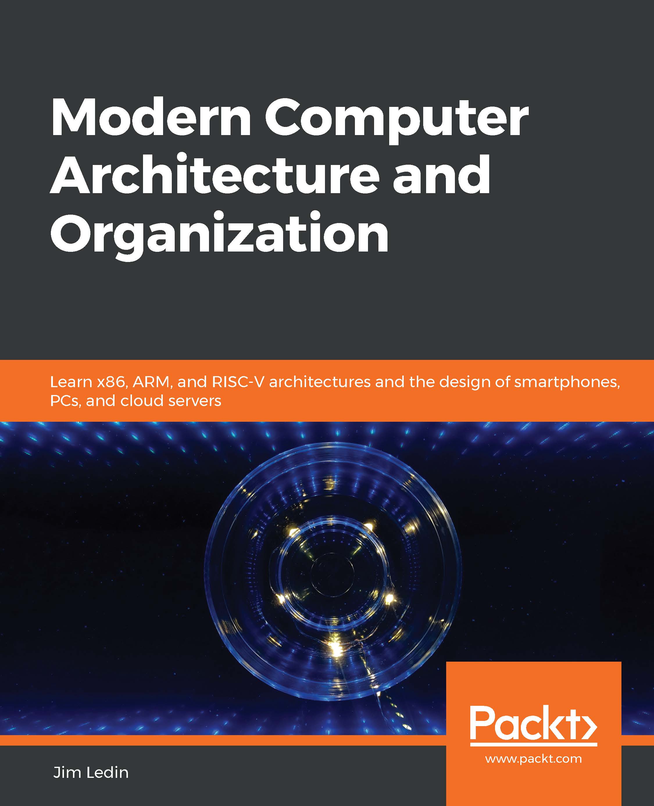
Modern Computer Architecture and Organization

Modern Computer Architecture and Organization: Learn x86, ARM, and RISC-V architectures and the design of smartphones, PCs, and cloud servers

eBook
€8.99 €29.99
Paperback
€37.99
Subscription
Free Trial
Renews at €18.99p/m

What do you get with eBook?

Product feature icon Instant access to your Digital eBook purchase
Product feature icon Download this book in EPUB and PDF formats
Product feature icon Access this title in our online reader with advanced features
Product feature icon DRM FREE - Read whenever, wherever and however you want
Product feature icon AI Assistant (beta) to help accelerate your learning
OR
Modal Close icon
Payment Processing...
tick Completed

Billing Address

Table of content icon View table of contents Preview book icon Preview Book

Modern Computer Architecture and Organization

Chapter 1: Introducing Computer Architecture

The architecture of automated computing devices has evolved from mechanical systems constructed nearly two centuries ago to the broad array of modern electronic computing technologies we use directly and indirectly every day. Along the way, there have been stretches of incremental technological improvement interspersed with disruptive advances that have drastically altered the trajectory of the industry. These trends can be expected to continue into the future.

In past decades, the 1980s, for example, students and technical professionals eager to learn about computing devices had a limited range of subject matter available for this purpose. If they had a computer of their own, it might have been an IBM PC or an Apple II. If they worked for an organization with a computing facility, they might have used an IBM mainframe or a Digital Equipment Corporation VAX minicomputer. These examples, and a limited number of similar systems, encompassed most people's exposure to computer systems of the time.

Today, numerous specialized computing architectures exist to address widely varying user needs. We carry miniature computers in our pockets and purses that can place phone calls, record video, and function as full participants on the Internet. Personal computers remain popular in a format outwardly similar to the PCs of past decades. Today's PCs, however, are orders of magnitude more capable than the first generations of PCs in terms of computing power, memory size, disk space, graphics performance, and communication capability.

Companies offering web services to hundreds of millions of users construct vast warehouses filled with thousands of closely coordinated computer systems capable of responding to a constant stream of requests with extraordinary speed and precision. Machine learning systems are trained through the analysis of enormous quantities of data to perform complex activities, such as driving automobiles.

This chapter begins by presenting a few key historical computing devices and the leaps in technology associated with them. This chapter will examine modern-day trends related to technological advances and introduce the basic concepts of computer architecture, including a close look at the 6502 microprocessor. These topics will be covered:

  • The evolution of automated computing devices
  • Moore's law
  • Computer architecture

The evolution of automated computing devices

This section reviews some classic machines from the history of automated computing devices and focuses on the major advances each embodied. Babbage's Analytical Engine is included here because of the many leaps of genius contained in its design. The other systems are discussed because they embodied significant technological advances and performed substantial real-world work over their lifetimes.

Charles Babbage's Analytical Engine

Although a working model of the Analytical Engine was never constructed, the detailed notes Charles Babbage developed from 1834 until his death in 1871 described a computing architecture that appeared to be both workable and complete. The Analytical Engine was intended to serve as a general-purpose programmable computing device. The design was entirely mechanical and was to be constructed largely of brass. It was designed to be driven by a shaft powered by a steam engine.

Borrowing from the punched cards of the Jacquard loom, the rotating studded barrels used in music boxes, and the technology of his earlier Difference Engine (also never completed in his lifetime, and more of a specialized calculating device than a computer), the Analytical Engine design was, otherwise, Babbage's original creation.

Unlike most modern computers, the Analytical Engine represented numbers in signed decimal form. The decision to use base-10 numbers rather than the base-2 logic of most modern computers was the result of a fundamental difference between mechanical technology and digital electronics. It is straightforward to construct mechanical wheels with ten positions, so Babbage chose the human-compatible base-10 format because it was not significantly more technically challenging than using some other number base. Simple digital circuits, on the other hand, are not capable of maintaining ten different states with the ease of a mechanical wheel.

All numbers in the Analytical Engine consisted of 40 decimal digits. The large number of digits was likely selected to reduce problems with numerical overflow. The Analytical Engine did not support floating-point mathematics.

Each number was stored on a vertical axis containing 40 wheels, with each wheel capable of resting in ten positions corresponding to the digits 0-9. A 41st number wheel contained the sign: any even number on this wheel represented a positive sign and any odd number represented a negative sign. The Analytical Engine axis was somewhat analogous to the register used in modern processors except the readout of an axis was destructive. If it was necessary to retain an axis's value after it had been read, another axis had to store a copy of the value. Numbers were transferred from one axis to another, or used in computations, by engaging a gear with each digit wheel and rotating the wheel to read out the numerical value. The axes serving as system memory were referred to collectively as the store.

The addition of two numbers used a process somewhat similar to the method of addition taught to schoolchildren. Assume a number stored on one axis, let's call it the addend, was to be added to a number on another axis, let's call it the accumulator. The machine would connect each addend digit wheel to the corresponding accumulator digit wheel through a train of gears. It would then simultaneously rotate each addend digit downward to zero while driving the accumulator digit an equivalent rotation in the increasing direction. If an accumulator digit wrapped around from nine to zero, the next most significant accumulator digit would increment by one. This carry operation would propagate across as many digits as needed (think of adding 1 to 999,999). By the end of the process, the addend axis would hold the value zero and the accumulator axis would hold the sum of the two numbers. The propagation of carries from one digit to the next was the most mechanically complex part of the addition process.

Operations in the Analytical Engine were sequenced by music box-like rotating barrels in a construct called the mill, which is analogous to the processing component of a modern CPU. Each Analytical Engine instruction was encoded in a vertical row of locations on the barrel where the presence or absence of a stud at a particular location either engaged a section of the Engine's machinery or left the state of that section unchanged. Based on Babbage's hypothesized execution speed, the addition of two 40-digit numbers, including the propagation of carries, would take about three seconds.

Babbage conceived several important concepts for the Engine that remain relevant today. His design supported a degree of parallel processing that accelerated the computation of series of values for output as numerical tables. Mathematical operations such as addition supported a form of pipelining, in which sequential operations on different data values overlapped in time.

Babbage was well aware of the complexities associated with mechanical devices such as friction, gear backlash, and wear over time. To prevent errors caused by these effects, the Engine incorporated mechanisms called lockings that were applied during data transfers across axes. The lockings forced the number wheels into valid positions and prevented accumulated errors from allowing a wheel to drift to an incorrect value. The use of lockings is analogous to the amplification of potentially weak input signals to produce stronger outputs by the digital logic gates in modern processors.

The Analytical Engine was programmed using punched cards and supported branching operations and nested loops. The most complex program for the Analytical Engine was developed by Ada Lovelace to compute the Bernoulli numbers.

Babbage constructed a trial model of a portion of the Analytical Engine mill, which is currently on display at the Science Museum in London.

ENIAC

ENIAC, the Electronic Numerical Integrator and Computer, was completed in 1945 and was the first programmable general-purpose electronic computer. The system consumed 150 kilowatts of electricity, occupied 1,800 square feet of floor space, and weighed 27 tons.

The design was based on vacuum tubes, diodes, and relays. ENIAC contained over 17,000 vacuum tubes that functioned as switching elements. Similar to the Analytical Engine, it used base-10 representation of ten-digit decimal numbers implemented using ten-position ring counters (the ring counter will be discussed in Chapter 2, Digital Logic). Input data was received from an IBM punch-card reader and the output of computations was sent to a card punch machine.

The ENIAC architecture was capable of complex sequences of processing steps including loops, branches, and subroutines. The system had 20 ten-digit accumulators that were similar to registers in modern computers. However, it did not initially have any memory storage beyond the accumulators. If intermediate values were required for use in later computations, they had to be written to punch cards and read back in when needed. ENIAC could perform about 385 multiplications per second.

ENIAC programs consisted of plugboard wiring and switch-based function tables. Programming the system was an arduous process that often took the team of talented female programmers weeks to complete. Reliability was a problem, as vacuum tubes failed regularly, requiring troubleshooting on a day-to-day basis to isolate and replace failed tubes.

In 1948, ENIAC was improved by adding the ability to program the system via punch cards rather than plugboards. This improvement greatly enhanced the speed with which programs could be developed. As a consultant for this upgrade, John von Neumann proposed a processing architecture based on a single memory region containing program instructions and data, a processing component with an arithmetic logic unit and registers, and a control unit with an instruction register and a program counter. Many modern processors continue to implement this general structure, now known as the von Neumann architecture.

Early applications of ENIAC included analyses related to the development of the hydrogen bomb and the computation of firing tables for long-range artillery.

IBM PC

In the years following the construction of ENIAC, several technological breakthroughs resulted in remarkable advances in computer architectures:

  • The invention of the transistor in 1947 by John Bardeen, Walter Brattain, and William Shockley delivered a vast improvement over the vacuum tube technology prevalent at the time. Transistors were faster, smaller, consumed less power, and, once production processes had been sufficiently optimized, were much more reliable than the failure-prone tubes.
  • The commercialization of integrated circuits in 1958, led by Jack Kilby of Texas Instruments, began the process of combining large numbers of formerly discrete components onto a single chip of silicon.
  • In 1971, Intel began production of the first commercially available microprocessor, the Intel 4004. The 4004 was intended for use in electronic calculators and was specialized to operate on 4-bit binary coded decimal digits.

From the humble beginning of the Intel 4004, microprocessor technology advanced rapidly over the ensuing decade by packing increasing numbers of circuit elements onto each chip and expanding the capabilities of the microprocessors implemented on the chips.

The 8088 microprocessor

IBM released the IBM PC in 1981. The original PC contained an Intel 8088 microprocessor running at a clock frequency of 4.77 MHz and featured 16 KB of RAM, expandable to 256 KB. It included one or, optionally, two floppy disk drives. A color monitor was also available. Later versions of the PC supported more memory, but because portions of the address space had been reserved for video memory and read-only memory, the architecture could support a maximum of 640 KB of RAM.

The 8088 contained fourteen 16-bit registers. Four were general purpose registers (AX, BX, CX, and DX.) Four were memory segment registers (CS, DS, SS, and ES) that extended the address space to 20 bits. Segment addressing functioned by adding a 16-bit segment register value, shifted left by four bit positions, to a 16-bit offset contained in an instruction to produce a physical memory address within a one megabyte range.

The remaining 8088 registers were the Stack Pointer (SP), the Base Pointer (BP), the Source Index (SI), the Destination Index (DI), the Instruction Pointer (IP), and the Status Flags (FLAGS). Modern x86 processers employ an architecture remarkably similar to this register set (Chapter 10, Modern Processor Architectures and Instruction Sets, will cover the details of the x86 architecture). The most obvious differences between the 8088 and x86 are the extension of the register widths to 32 bits in x86 and the addition of a pair of segment registers (FS and GS) that are used today primarily as data pointers in multithreaded operating systems.

The 8088 had an external data bus width of 8 bits, which meant it took two bus cycles to read or write a 16-bit value. This was a performance downgrade compared to the earlier 8086 processor, which employed a 16-bit external bus. However, the use of the 8-bit bus made the PC more economical to produce and provided compatibility with lower-cost 8-bit peripheral devices. This cost-sensitive design approach helped to reduce the purchase price of the PC to a level accessible to more potential customers.

Program memory and data memory shared the same address space, and the 8088 accessed memory over a single bus. In other words, the 8088 implemented the von Neumann architecture. The 8088 instruction set included instructions for data movement, arithmetic, logical operations, string manipulation, control transfer (conditional and unconditional jumps and subroutine call and return), input/output, and additional miscellaneous functions. The processor required about 15 clock cycles per instruction on average, resulting in an execution speed of 0.3 million instructions per second (MIPS).

The 8088 supported nine distinct modes for addressing memory. This variety of modes was needed to efficiently implement methods for accessing a single item at a time as well as for iterating through sequences of data.

The segment registers in the 8088 architecture provided a clever way to expand the range of addressable memory without increasing the length of most instructions referencing memory locations. Each segment register allowed access to a 64-kilobyte block of memory beginning at a physical memory address defined at a multiple of 16 bytes. In other words, the 16-bit segment register represented a 20-bit base address with the lower four bits set to zero. Instructions could then reference any location within the 64-kilobyte segment using a 16-bit offset from the address defined by the segment register.

The CS register selected the code segment location in memory and was used in fetching instructions and performing jumps and subroutine calls and returns. The DS register defined the data segment location for use by instructions involving the transfer of data to and from memory. The SS register set the stack segment location, which was used for local memory allocation within subroutines and for storing subroutine return addresses.

Programs that required less than 64-kilobyte in each of the code, data, and stack segments could ignore the segment registers entirely because those registers could be set once at program startup (compilers would do this automatically) and remain unchanged through execution. Easy!

Things got quite a bit more complicated when a program's data size increased beyond 64-kilobyte. Compilers for the 8088 architecture distinguished between near and far references to memory. A near pointer represented a 16-bit offset from the current segment register base address. A far pointer contained 32 bits of addressing information: a 16-bit segment register value and a 16-bit offset. Far pointers obviously required 16 bits of extra data memory and they required additional processing time. Making a single memory access using a far pointer involved the following steps:

  1. Save the current segment register contents to a temporary location.
  2. Load the new segment value into the register.
  3. Access the data (read or write as needed) using an offset from the segment base.
  4. Restore the original segment register value.

When using far pointers, it was possible to declare data objects (for example, an array of characters) up to 64 KB in size. If you needed a larger structure, you had to work out how to break it into chunks no larger than 64 KB and manage them yourself. As a result of these segment register manipulations, programs that required extensive access to data larger than 64 KB were susceptible to code size bloat and slower execution.

The IBM PC motherboard also contained a socket for an optional Intel 8087 floating-point coprocessor. The designers of the 8087 invented data formats and processing rules for 32-bit and 64-bit floating point numbers that became enshrined in 1985 as the IEEE 754 floating-point standard, which remains in near-universal use today. The 8087 could perform about 50,000 floating-point operations per second. We will look at floating-point processors in detail in Chapter 9, Specialized Processor Extensions.

The 80286 and 80386 microprocessors

The second generation of the IBM PC, the PC AT, was released in 1984. AT stood for Advanced Technology and referred to several significant enhancements over the original PC that mostly resulted from the use of the Intel 80286 processor.

Like the 8088, the 80286 was a 16-bit processor, and it maintained backward compatibility with the 8088: 8088 code could run unmodified on the 80286. The 80286 had a 16-bit data bus and 24 address lines supporting a 16-megabyte address space. The external data bus width was 16 bits, improving data access performance over the 8-bit bus of the 8088. The instruction execution rate (instructions per clock cycle) was about double the 8088 in many applications. This meant that at the same clock speed the 80286 would be twice as fast as the 8088. The original PC AT clocked the processor at 6 MHz and a later version operated at 8 MHz. The 6 MHz variant of the 80286 achieved an instruction execution rate of about 0.9 MIPS.

The 80286 implemented a protected virtual address mode intended to support multiuser operating systems and multitasking. In protected mode, the processor enforced memory protection to ensure one user's programs could not interfere with the operating system or with other users' programs. This groundbreaking technological advance remained little used for many years, mainly because of the prohibitive cost of adding sufficient memory to a computer system to make it useful in a multiuser, multitasking context.

The next generation of the x86 processor line was the 80386, introduced in 1985. The 80386 was a 32-bit processor with support for a flat 32-bit memory model in protected mode. The flat memory model allowed programmers to address up to 4 GB directly, without the need to manipulate segment registers. Compaq introduced an IBM PC-compatible personal computer based on the 80386 called the DeskPro in 1986. The DeskPro shipped with a version of Microsoft Windows targeted to the 80386 architecture.

The 80386 maintained a large degree of backward compatibility with the 80286 and 8088 processors. The design implemented in the 80386 remains the current standard x86 architecture. Much more about this architecture will be covered in Chapter 10, Modern Processor Architectures and Instruction Sets.

The initial version of the 80386 was clocked at 33 MHz and achieved about 11.4 MIPS. Modern implementations of the x86 architecture run several hundred times faster than the original as the result of higher clock speeds, performance enhancements such as extensive use of cache memory, and more efficient instruction execution at the hardware level.

The iPhone

In 2007, Steve Jobs introduced the iPhone to a world that had no idea it had any use for such a device. The iPhone built upon previous revolutionary advances from Apple Computer including the Macintosh computer in 1984 and the iPod music player in 2001. The iPhone combined the functions of the iPod, a mobile telephone, and an Internet-connected computer.

The iPhone did away with the hardware keyboard that was common on smartphones of the time and replaced it with a touchscreen capable of displaying an on-screen keyboard or any other type of user interface. The screen was driven by the user's fingers and supported multi-finger gestures for actions such as zooming a photo.

The iPhone ran the OS X operating system, the same OS used on the flagship Macintosh computers of the time. This decision immediately enabled the iPhone to support a vast range of applications already developed for Macs and empowered software developers to rapidly introduce new applications tailored to the iPhone, once Apple began allowing third-party application development.

The iPhone 1 had a 3.5" screen with a resolution of 320x480 pixels. It was 0.46 inches thick (thinner than other smartphones), had a 2-megapixel camera built in, and weighed 4.8 oz. A proximity sensor detected when the phone was held to the user's ear and turned off screen illumination and touchscreen sensing during calls. It had an ambient light sensor to automatically set the screen brightness and an accelerometer detected whether the screen was being held in portrait or landscape orientation.

The iPhone 1 included 128 MB of RAM, 4 GB, 8 GB, or 16 GB of flash memory, and supported Global System for Mobile communications (GSM) cellular communication, Wi-Fi (802.11b/g), and Bluetooth.

In contrast to the abundance of openly available information about the IBM PC, Apple was notoriously reticent about releasing the architectural details of the iPhone's construction. Apple released no information about the processor or other internal components of the first iPhone, simply calling it a closed system.

Despite the lack of official information from Apple, other parties have enthusiastically torn down the various iPhone models and attempted to identify the phone's components and how they interconnect. Software sleuths have devised various tests to attempt to determine the specific processor model and other digital devices implemented in the iPhone. These reverse engineering efforts are subject to error, so descriptions of the iPhone architecture in this section should be taken with a grain of salt.

The iPhone 1 processor was a 32-bit ARM11 manufactured by Samsung running at 412 MHz. The ARM11 was an improved variant of previous generation ARM processors and included an 8-stage instruction pipeline and support for Single Instruction-Multiple Data (SIMD) processing to improve audio and video performance. The ARM processor architecture will be discussed further in Chapter 10, Modern Processor Architectures and Instruction Sets.

The iPhone 1 was powered by a 3.7V lithium-ion polymer battery. The battery was not intended to be replaceable, and Apple estimated it would lose about 20 percent of its original capacity after 400 charge and discharge cycles. Apple quoted up to 250 hours of standby time and 8 hours of talk time on a single charge.

Six months after the iPhone was introduced, Time magazine named the iPhone the "Invention of the Year" for 2007. In 2017, Time ranked the 50 Most Influential Gadgets of All Time. The iPhone topped the list.

Moore's law

For those working in the rapidly advancing field of computer technology, it is a significant challenge to make plans for the future. This is true whether the goal is to plot your own career path or for a giant semiconductor corporation to identify optimal R&D investments. No one can ever be completely sure what the next leap in technology will be, what effects from it will ripple across the industry and its users, or when it will happen. One technique that has proven useful in this difficult environment is to develop a rule of thumb, or empirical law, based on experience.

Gordon Moore co-founded Fairchild Semiconductor in 1957 and was later the chairman and CEO of Intel. In 1965, Moore published an article in Electronics magazine in which he offered his prediction of the changes that would occur in the semiconductor industry over the following ten years. In the article, he observed that the number of formerly discrete components such as transistors, diodes, and capacitors that could be integrated onto a single chip had been doubling approximately yearly and the trend was likely to continue over the subsequent ten years. This doubling formula came to be known as Moore's law. This was not a scientific law in the sense of the law of gravity. Rather, it was based on observation of historical trends, and he believed this formulation had some ability to predict the future.

Moore's law turned out to be impressively accurate over those ten years. In 1975, he revised the predicted growth rate for the following ten years to doubling the number of components per integrated circuit every two years rather than yearly. This pace continued for decades, up until about 2010. In more recent years, the growth rate has appeared to decline slightly. In 2015, Brian Krzanich, Intel CEO, stated that the company's growth rate had slowed to doubling about every two and a half years.

Despite the fact that the time to double integrated circuit density is increasing, the current pace represents a phenomenal rate of growth that can be expected to continue into the future, just not quite as rapidly as it once progressed.

Moore's law has proven to be a reliable tool for evaluating the performance of semiconductor companies over the decades. Companies have used it to set goals for the performance of their products and to plan their investments. By comparing the integrated circuit density increases for a company's products against prior performance, and against other companies, it is possible for semiconductor executives and industry analysts to evaluate and score company performance. The results of these analyses have fed directly into decisions to build enormous new fabrication plants and to push the boundaries of ever-smaller integrated circuit feature sizes.

The decades since the introduction of the IBM PC have seen tremendous growth in the capability of single-chip microprocessors. Current processor generations are hundreds of times faster, operate on 32-bit and 64-bit data natively, have far more integrated memory resources, and unleash vastly more functionality, all packed into a single integrated circuit.

The increasing density of semiconductor features, as predicted by Moore's law, has enabled all of these improvements. Smaller transistors run at higher clock speeds due to the shorter connection paths between circuit elements. Smaller transistors also, obviously, allow more functionality to be packed into a given amount of die area. Being smaller and closer to neighboring components allows the transistors to consume less power and generate less heat.

There was nothing magical about Moore's law. It was an observation of the trends in progress at the time. One trend was the steadily increasing size of semiconductor dies. This was the result of improving production processes that reduced the density of defects, hence allowing acceptable production yield with larger integrated circuit dies. Another trend was the ongoing reduction in the size of the smallest components that could be reliably produced in a circuit. The final trend was what Moore referred to as the "cleverness" of circuit designers in making increasingly efficient and effective use of the growing number of circuit elements placed on a chip.

Traditional semiconductor manufacturing processes have begun to approach physical limits that will eventually put the brakes on growth under Moore's law. The smallest features on current commercially available integrated circuits are around 10 nanometers (nm). For comparison, a typical human hair is about 50,000 nm thick and a water molecule (one of the smallest molecules) is 0.28 nm across. There is a point beyond which it is simply not possible for circuit elements to become smaller as the sizes approach atomic scale.

In addition to the challenge of building reliable circuit components from a small number of molecules, other physical effects with names such as Abbe diffraction limit become significant impediments to single-digit nanometer-scale circuit production. We won't get into the details of these phenomena; it's sufficient to know the steady increase in integrated circuit component density that has proceeded for decades under Moore's law is going to become a lot harder to continue over the next few years.

This does not mean we will be stuck with processors essentially the same as those that are now commercially available. Even as the rate of growth in transistor density slows, semiconductor manufacturers are pursuing several alternative methods to continue growing the power of computing devices. One approach is specialization, in which circuits are designed to perform a specific category of tasks extremely well rather than performing a wide variety of tasks merely adequately.

Graphical Processing Units (GPUs) are an excellent example of specialization. Original GPUs focused exclusively on improving the speed at which three-dimensional graphics scenes could be rendered, mostly for use in video gaming. The calculations involved in generating a three-dimensional scene are well defined and must be applied to thousands of pixels to create a single frame. The process must be repeated for each subsequent frame, and frames may need to be redrawn at a 60 Hz or higher rate to provide a satisfactory user experience. The computationally demanding and repetitive nature of this task is ideally suited for acceleration via hardware parallelism. Multiple computing units within a GPU simultaneously perform essentially the same calculations on different input data to produce separate outputs. Those outputs are combined to generate the final scene. Modern GPU designs have been enhanced to support other domains, such as training neural networks on massive amounts of data. GPUs will be covered in detail in Chapter 6, Specialized Computing Domains.

As Moore's law shows signs of beginning to fade over the coming years, what advances might take its place to kick off the next round of innovations in computer architectures? We don't know for sure today, but some tantalizing options are currently under intense study. Quantum computing is one example of these technologies. We will cover that technology in Chapter 14, Future Directions in Computer Architectures.

Quantum computing takes advantage of the properties of subatomic particles to perform computations in a manner that traditional computers cannot. A basic element of quantum computing is the qubit, or quantum bit. A qubit is similar to a regular binary bit, but in addition to representing the states 0 and 1, qubits can attain a state that is a superposition of the 0 and 1 states. When measured, the qubit output will always be 0 or 1, but the probability of producing either output is a function of the qubit's quantum state prior to being read. Specialized algorithms are required to take advantage of the unique features of quantum computing.

Another possibility is that the next great technological breakthrough in computing devices will be something that we either haven't thought of, or if we did think about it, we may have dismissed the idea out of hand as unrealistic. The iPhone, discussed in the preceding section, is an example of a category-creating product that revolutionized personal communication and enabled use of the Internet in new ways. The next major advance may be a new type of product, a surprising new technology, or some combination of product and technology. Right now, we don't know what it will be or when it will happen, but we can say with confidence that such changes are coming.

Computer architecture

The descriptions of a small number of key architectures from the history of computing mentioned in the previous section included some terms that may or may not be familiar to you. This section will provide an introduction to the building blocks used to construct modern-day processors and related computer subsystems.

One ubiquitous feature of modern computers is the use of voltage levels to indicate data values. In general, only two voltage levels are recognized: a low level and a high level. The low level is often assigned the value zero and the high level assigned the value one. The voltage at any point in a circuit (digital or otherwise) is analog in nature and can take on any voltage within its operating range. When changing from the low level to the high level, or vice versa, the voltage must pass through all voltages in between. In the context of digital circuitry, the transitions between low and high levels happen quickly and the circuitry is designed to not react to voltages between the high and low levels.

Binary and hexadecimal numbers

The circuitry within a processor does not work directly with numbers, in any sense. Processor circuit elements obey the laws of electricity and electronics and simply react to the inputs provided to them. The inputs that drive these actions result from the code developed by programmers and from the data provided as input to the program. The interpretation of the output of a program as, say, numbers in a spreadsheet, or characters in a word processing program, is a purely human interpretation that assigns meaning to the result of the electronic interactions within the processor. The decision to assign zero to the low voltage and one to the high voltage is the first step in the interpretation process.

The smallest unit of information in a digital computer is a binary digit, called a bit, which represents a discrete data element containing the value zero or one. A number of bits can be placed together to enable representation of a greater range of values. A byte is composed of eight bits placed together to form a single value. The byte is the smallest unit of information that can be read from or written to memory by most modern processors.

A single bit can take on two values: 0 and 1. Two bits placed together can take on four values: 00, 01, 10, and 11. Three bits can take on eight values: 000, 001, 010, 011, 100, 101, 110, and 111. In fact, any number of bits, n, can take on 2n values, where 2n indicates multiplying n copies of two together. An 8-bit byte, therefore, can take on 28 or 256 different values.

The binary number format is not most people's first choice when it comes to performing arithmetic, and working with numbers such as 11101010 can be confusing and error prone, especially when dealing with 32- and 64-bit values. To make working with these numbers somewhat easier, hexadecimal numbers are often used instead. The term hexadecimal is often shortened to hex. In the hexadecimal number system, binary numbers are separated into groups of four bits. Since there are four bits in the group, the number of possible values is 24, or 16. The first ten of these 16 numbers are assigned the digits 0-9. The last six are assigned the letters A-F. Table 1.1 shows the first 16 binary values starting at zero along with the corresponding hexadecimal digit and the decimal equivalent to the binary and hex values.

Table 1.1: Binary, hexadecimal, and decimal numbers

The binary number 11101010 can be represented more compactly by breaking it into two 4-bit groups (1110 and 1010) and writing them as the hex digits EA. Because binary digits can take on only two values, binary is a base-2 number system. Hex digits can take on 16 values, so hexadecimal is base-16. Decimal digits can have ten values, therefore decimal is base-10.

When working with these different number bases, it is possible for things to become confusing. Is the number written as 100 a binary, hexadecimal, or decimal value? Without additional information, you can't tell. Various programming languages and textbooks have taken different approaches to remove this ambiguity. In most cases, decimal numbers are unadorned, so the number 100 is usually decimal. In programming languages such as C and C++, hexadecimal numbers are prefixed by 0x so the number 0x100 is 100 hex. In assembly languages, either the prefix character $, or the suffix h might be used to indicate hexadecimal numbers. The use of binary values in programming is less common, mostly because hexadecimal is preferred due to its compactness. Some compilers support the use of 0b as a prefix for binary numbers.

Hexadecimal number representation

This book uses either the prefix $ or the suffix h to represent hexadecimal numbers, depending on the context. The suffix b will represent binary numbers, and the absence of a prefix or suffix indicates decimal numbers.

Bits are numbered individually within a binary number, with bit zero as the rightmost, least significant bit. Bit numbers increase in magnitude leftward. Some examples should make this clear: In Table 1.1, the binary value 0001b (1 decimal) has bit number zero set and the remaining three bits are cleared. In 0010b (2 decimal), bit 1 is set and the other bits are cleared. In 0100b (4 decimal), bit 2 is set and the other bits are cleared.

Set versus cleared

A bit that is set has the value 1. A bit that is cleared has the value 0.

An 8-bit byte can take on values from $00h to $FF, equivalent to the decimal range 0-255. When performing addition at the byte level, it is possible for the result to exceed 8 bits. For example, adding $01 to $FF results in the value $100. When using 8-bit registers, this represents a carry, which must be handled appropriately.

In unsigned arithmetic, subtracting $01 from $00 results in a value of $FF. This constitutes a wraparound to $FF. Depending on the computation being performed, this may or may not be the desired result.

When desired, negative values can be represented using binary numbers. The most common signed number format in modern processors is two's complement. In two's complement, 8-bit signed numbers span the range from -128 to 127. The most significant bit of a two's complement data value is the sign bit: a 0 in this bit represents a positive value and a 1 represents a negative value. A two's complement number can be negated (multiplied by -1) by inverting all of the bits, adding 1, and ignoring any carry. Inverting a bit means changing a 0 bit to 1 and a 1 bit to 0.

Table 1.2: Negation operation examples

Note that negating zero returns a result of zero, as you would expect mathematically.

Two's complement arithmetic

Two's complement arithmetic is identical to unsigned arithmetic at the bit level. The manipulations involved in addition and subtraction are the same whether the input values are intended to be signed or unsigned. The interpretation of the result as signed or unsigned depends entirely on the intent of the user.

Table 1.3: Signed and unsigned 8-bit numbers

Signed and unsigned representations of binary numbers extend to larger integer data types. 16-bit values can represent unsigned integers from 0 to 65,535 and signed integers in the range -32,768 to 32,767. 32-bit, 64-bit, and even larger integer data types are commonly available in modern programming languages.

The 6502 microprocessor

This section will introduce the architecture of a processor with a relatively simple design compared to more powerful modern processors. The intent here is to provide a whirlwind introduction to some basic concepts shared by processors spanning the spectrum from the very low end to sophisticated modern processors.

The 6502 processor was introduced by MOS Technology in 1975. The 6502 found widespread use in its early years in video game consoles from Atari and Nintendo and in computers marketed by Commodore and Apple. The 6502 continues in widespread use today in embedded systems, with estimates of between five and ten billion (yes, billion) units produced as of 2018. In popular culture, both Bender the robot in Futurama and the T-800 robot in The Terminator appear to have employed the 6502, based on onscreen evidence.

Many early microprocessors, like the 6502, were powered by a constant voltage of 5 volts (5V). In these circuits, a low signal level is any voltage between 0 and 0.8V. A high signal level is any voltage between 2 and 5V. The low signal level is defined as logical 0 and the high signal level is defined as logical 1. Chapter 2, Digital Logic, will delve further into digital electronics.

The word length of a processor defines the size of the fundamental data element the processor operates upon. The 6502 has a word length of 8 bits. This means the 6502 reads and writes memory 8 bits at a time and stores data internally in 8-bit wide registers.

Program memory and data memory share the same address space and the 6502 accesses its memory over a single bus. As was the case with the Intel 8088, the 6502 implements the von Neumann architecture. The 6502 has a 16-bit address bus, enabling access to 64 KB of memory.

One kilobyte (abbreviated KB) is defined as 210, or 1,024 bytes. The number of unique binary combinations of the 16 address lines is 216, equal to 64 multiplied by 1,024, or 65,536 locations. Note that just because a device can address 64 KB, it does not mean there must be memory at all of those locations. The Commodore VIC-20, based on the 6502, contained just 5 KB of Random Access Memory (RAM) and 20 KB of Read-Only Memory (ROM).

The 6502 contains internal storage areas called registers. A register is a location in a logical device in which a word of information can be stored and acted upon during computation. A typical processor contains a small number of registers for temporarily storing data values and performing operations such as addition or address computation.

The following figure 1.1 shows the 6502 register structure. The processor contains five 8-bit registers (A, X, Y, P, and S) and one 16-bit register (PC). The numbers above each register indicate the bit numbers at each end of the register:

Figure 1.1: The 6502 register structure

Figure 1.1: 6502 register set

Each of the A, X, and Y registers can serve as a general-purpose storage location. Program instructions can load a value into one of those registers and, some instructions later, use the saved value for some purpose, as long as the intervening instructions did not modify the register contents. The A register is the only register capable of performing arithmetic operations. The X and Y registers, but not the A register, can be used as index registers in calculating memory addresses.

The P register contains processor flags. Each bit in this register has a unique purpose, except for the bit labeled 1. The 1 bit is unused and can be ignored. Each of the remaining bits in this register is called a flag and indicates a specific condition that has occurred or represents a configuration setting. The 6502 flags are as follows:

  • N: Negative sign flag: This flag is set when the result of an arithmetic operation sets bit 7 in the result. This flag is used in signed arithmetic.
  • V: Overflow flag: This flag is set when a signed addition or subtraction results in overflow or underflow outside the range -128 to 127.
  • B: Break flag: This flag indicates a Break (BRK) instruction has executed. This bit is not present in the P register itself. The B flag value is only relevant when examining the P register contents as stored onto the stack by a BRK instruction or by an interrupt. The B flag is set to distinguish a software interrupt resulting from a BRK instruction from a hardware interrupt during interrupt processing.
  • D: Decimal mode flag: This flag indicates processor arithmetic will operate in Binary-Coded Decimal (BCD) mode. BCD mode is rarely used and won't be discussed here, other than to note that this base-10 computation mode evokes the architectures of the Analytical Engine and ENIAC.
  • I: Interrupt disable flag: This flag indicates that interrupt inputs (other than the non-maskable interrupt) will not be processed.
  • Z: Zero flag: This flag is set when an operation produces a result of zero.
  • C: Carry flag: This flag is set when an arithmetic operation produces a carry.

The N, V, Z, and C flags are the most important flags in the context of general computing involving loops, counting, and arithmetic.

The S register is the stack pointer. In the 6502, the stack is the region of memory from addresses $100 to $1FF. This 256-byte range is used for temporary storage of parameters within subroutines and holds the return address when a subroutine is called. At system startup, the S register is initialized to point to the top of this range. Values are "pushed" onto the stack using instructions such as PHA, which pushes the contents of the A register onto the stack. When a value is pushed onto the stack, the 6502 stores the value at the address indicated by the S register, after adding the fixed $100 offset, then decrements the S register. Additional values can be placed on the stack by executing more push instructions. As additional values are pushed, the stack grows downward in memory. Programs must take care not to exceed the fixed 256-byte size of the stack when pushing data onto it.

Data stored on the stack must be retrieved in the reverse of the order from which it was pushed onto the stack. The stack is a Last-In, First-Out (LIFO) data structure, meaning when you "pop" a value from the stack, it is the byte most recently pushed onto it. The PLA instruction increments the S register by one, then copies the value at the address indicated by the S register (plus the $100 offset) into the A register.

The PC register is the program counter. This register contains the memory address of the next instruction to be executed. Unlike the other registers, the PC is 16 bits long, allowing access to the entire 6502 address space. Each instruction consists of a 1-byte operation code, called opcode for short, and may be followed by zero to two operand bytes, depending on the instruction. After each instruction executes, the PC updates to point to the next instruction following the one that just completed. In addition to these automatic updates during sequential instruction execution, the PC can be modified by jump instructions, branch instructions, and subroutine call and return instructions.

The 6502 instruction set

Each of the 6502 instructions has a three-character mnemonic. In assembly language source files, each line of code contains an instruction mnemonic followed by any operands associated with the instruction. The combination of the mnemonic and the operands defines the addressing mode. The 6502 supports several addressing modes providing a great deal of flexibility in accessing data in registers and memory. For this introduction, we'll only work with the immediate addressing mode, in which the operand itself contains a value rather than indicating a register or memory location containing the value. An immediate value is preceded by a # character.

In 6502 assembly, decimal numbers have no adornment (48 means 48 decimal) while hexadecimal values are preceded by a $ character ($30 means 30 hexadecimal, equivalent to 00110000b and to 48 decimal). An immediate decimal value looks like #48 and an immediate hexadecimal value looks like #$30.

Some assembly code examples will demonstrate the 6502 arithmetic capabilities. Five 6502 instructions are used in the following examples:

  • LDA loads register A with a value.
  • ADC performs addition using the Carry (C flag) as an additional input and output.
  • SBC performs subtraction using the Carry flag as an additional input and output.
  • SEC sets the Carry flag directly.
  • CLC clears the Carry flag directly.

Since the Carry flag is an input to the addition and subtraction instructions, it is important to ensure it has the correct value prior to executing the ADC or SBC instructions. Before initiating an addition operation, the C flag must be clear to indicate there is no carry from a prior addition. When performing multi-byte additions (say, with 16-bit, 32-bit, or 64-bit numbers), the carry, if any, will propagate from the sum of one byte pair to the next as you add the more significant bytes to each other. If the C flag is set when the ADC instruction executes, the effect is to add one to the result. After the ADC completes, the C flag serves as the ninth bit of the result: a C flag result of 0 means there was no carry, and a 1 indicates there was a carry from the 8-bit register.

Subtraction using the SBC instruction tends to be a bit more confusing to novice 6502 assembly language programmers. Schoolchildren learning subtraction use the technique of borrowing when subtracting a larger digit from a smaller digit. In the 6502, the C flag represents the opposite of Borrow. If C is 1, then Borrow is 0, and if C is 0, Borrow is 1. Performing a simple subtraction with no incoming Borrow requires setting the C flag before executing the SBC command.

The examples in the following employ the 6502 as a calculator using inputs defined directly in the code and with the result stored in the A register. The Results columns show the final value of the A register and the N, V, Z, and C flags.

Table 1.4: 6502 arithmetic instruction sequences

If you don't happen to have a 6502-based computer with an assembler and debugger handy, there are several free 6502 emulators available online that you can run in your web browser. One excellent emulator is at https://skilldrick.github.io/easy6502/. Visit the website and scroll down until you find a default code listing with buttons for assembling and running 6502 code. Replace the default code listing with a group of three instructions from Table 1.4, then assemble the code. To examine the effect of each instruction in the sequence, use the debugger controls to single-step through the instructions and observe the result of each instruction on the processor registers.

This section has provided a very brief introduction to the 6502 processor and a small subset of its capabilities. One point of this analysis was to illustrate the challenge of dealing simply with the issue of carries when performing addition and borrows when doing subtraction. From Charles Babbage to the designers of the 6502, computer architects have developed solutions to the problems of computation and implemented them using the best technology available to them.

Summary

This chapter began with a brief history of automated computing devices and described significant technological advances that drove leaps in computational capability. A discussion of Moore's law was followed with an assessment of its applicability over previous decades and implications for the future. The basic concepts of computer architecture were introduced through a discussion of the 6502 microprocessor. The history of computer architecture is fascinating, and I encourage you to explore it further.

The next chapter will introduce digital logic, beginning with the properties of basic electrical circuits and proceeding through the design of digital subsystems used in modern processors. You will learn about logic gates, flip-flops, and digital circuits including multiplexers, shift registers, and adders. It includes an introduction to hardware description languages, which are specialized computer languages used in the design of complex digital devices such as computer processors.

Exercises

  1. Using your favorite programming language, develop a simulation of a single-digit decimal adder that operates in the same manner as in Babbage's Analytical Engine. First, prompt the user for two digits in the range 0-9: the addend and the accumulator. Display the addend, the accumulator, and the carry, which is initially zero. Perform a series of cycles as follows:

    a. If the addend is zero, display the values of the addend, accumulator, and carry and terminate the program.

    b. Decrement the addend by one and increment the accumulator by one.

    c. If the accumulator incremented from nine to zero, increment the carry.

    d. Go back to step a.

    Test your code with these sums: 0+0, 0+1, 1+0, 1+2, 5+5, 9+1, and 9+9.

  2. Create arrays of 40 decimal digits each for the addend, accumulator, and carry. Prompt the user for two decimal integers of up to 40 digits each. Perform the addition digit by digit using the cycles described in Exercise 1, and collect the carry output from each digit position in the carry array. After the cycles are complete, insert carries, and, where necessary, ripple them across digits to complete the addition operation. Display the results after each cycle and at the end. Test with the same sums as in Exercise 1 and test 99+1, 999999+1, 49+50, and 50+50.
  3. Modify the program of Exercise 2 to implement subtraction of 40-digit decimal values. Perform borrowing as required. Test with 0-0, 1-0, 1000000-1, and 0-1. What is the result for 0-1?
  4. 6502 assembly language references data in memory locations using an operand value containing the address (without the # character that indicates an immediate value). For example, the LDA $00 instruction loads the byte at memory address $00 into A. STA $01 stores the byte in A into address $01. Addresses can be any value in the range 0 to $FFFF, assuming memory exists at the address and the address is not already in use for some other purpose. Using your preferred 6502 emulator, write 6502 assembly code to store a 16-bit value into addresses $00-$01, store a second value into addresses $02-$03, then add the two values and store the result in $04-$05. Be sure to propagate any carry between the two bytes. Ignore any carry from the 16-bit result. Test with $0000+$0001, $00FF+$0001, and $1234+$5678.
  5. Write 6502 assembly code to subtract two 16-bit values in a manner similar to Exercise 4. Test with $0001-$0000, $0001-$0001, $0100-$00FF, and $0000-$0001. What is the result for $0000-$0001?
  6. Write 6502 assembly code to store two 32-bit integers to addresses $00-03 and $04-$07, then add them, storing the results in $08-$0B. Use a looping construct, including a label and a branch instruction, to iterate over the bytes of the two values to be added. Search the Internet for the details of the 6502 decrement and branch instructions and the use of labels in assembly language. Hint: The 6502 zero-page indexed addressing mode works well in this application.
Left arrow icon Right arrow icon
Download code icon Download Code

Key benefits

  • Understand digital circuitry with the help of transistors, logic gates, and sequential logic
  • Examine the architecture and instruction sets of x86, x64, ARM, and RISC-V processors
  • Explore the architecture of modern devices such as the iPhone X and high-performance gaming PCs

Description

Are you a software developer, systems designer, or computer architecture student looking for a methodical introduction to digital device architectures but overwhelmed by their complexity? This book will help you to learn how modern computer systems work, from the lowest level of transistor switching to the macro view of collaborating multiprocessor servers. You'll gain unique insights into the internal behavior of processors that execute the code developed in high-level languages and enable you to design more efficient and scalable software systems. The book will teach you the fundamentals of computer systems including transistors, logic gates, sequential logic, and instruction operations. You will learn details of modern processor architectures and instruction sets including x86, x64, ARM, and RISC-V. You will see how to implement a RISC-V processor in a low-cost FPGA board and how to write a quantum computing program and run it on an actual quantum computer. By the end of this book, you will have a thorough understanding of modern processor and computer architectures and the future directions these architectures are likely to take.

Who is this book for?

This book is for software developers, computer engineering students, system designers, reverse engineers, and anyone looking to understand the architecture and design principles underlying modern computer systems from tiny embedded devices to warehouse-size cloud server farms. A general understanding of computer processors is helpful but not required.

What you will learn

  • Get to grips with transistor technology and digital circuit principles
  • Discover the functional elements of computer processors
  • Understand pipelining and superscalar execution
  • Work with floating-point data formats
  • Understand the purpose and operation of the supervisor mode
  • Implement a complete RISC-V processor in a low-cost FPGA
  • Explore the techniques used in virtual machine implementation
  • Write a quantum computing program and run it on a quantum computer

Product Details

Country selected
Publication date, Length, Edition, Language, ISBN-13
Publication date : Apr 30, 2020
Length: 560 pages
Edition : 1st
Language : English
ISBN-13 : 9781838987107

What do you get with eBook?

Product feature icon Instant access to your Digital eBook purchase
Product feature icon Download this book in EPUB and PDF formats
Product feature icon Access this title in our online reader with advanced features
Product feature icon DRM FREE - Read whenever, wherever and however you want
Product feature icon AI Assistant (beta) to help accelerate your learning
OR
Modal Close icon
Payment Processing...
tick Completed

Billing Address

Product Details

Publication date : Apr 30, 2020
Length: 560 pages
Edition : 1st
Language : English
ISBN-13 : 9781838987107

Packt Subscriptions

See our plans and pricing
Modal Close icon
€18.99 billed monthly
Feature tick icon Unlimited access to Packt's library of 7,000+ practical books and videos
Feature tick icon Constantly refreshed with 50+ new titles a month
Feature tick icon Exclusive Early access to books as they're written
Feature tick icon Solve problems while you work with advanced search and reference features
Feature tick icon Offline reading on the mobile app
Feature tick icon Simple pricing, no contract
€189.99 billed annually
Feature tick icon Unlimited access to Packt's library of 7,000+ practical books and videos
Feature tick icon Constantly refreshed with 50+ new titles a month
Feature tick icon Exclusive Early access to books as they're written
Feature tick icon Solve problems while you work with advanced search and reference features
Feature tick icon Offline reading on the mobile app
Feature tick icon Choose a DRM-free eBook or Video every month to keep
Feature tick icon PLUS own as many other DRM-free eBooks or Videos as you like for just €5 each
Feature tick icon Exclusive print discounts
€264.99 billed in 18 months
Feature tick icon Unlimited access to Packt's library of 7,000+ practical books and videos
Feature tick icon Constantly refreshed with 50+ new titles a month
Feature tick icon Exclusive Early access to books as they're written
Feature tick icon Solve problems while you work with advanced search and reference features
Feature tick icon Offline reading on the mobile app
Feature tick icon Choose a DRM-free eBook or Video every month to keep
Feature tick icon PLUS own as many other DRM-free eBooks or Videos as you like for just €5 each
Feature tick icon Exclusive print discounts

Frequently bought together


Stars icon
Total 117.97
40 Algorithms Every Programmer Should Know
€37.99
Modern Computer Architecture and Organization
€37.99
Solutions Architect's Handbook
€41.99
Total 117.97 Stars icon
Banner background image

Table of Contents

19 Chapters
Section 1: Fundamentals of Computer Architecture Chevron down icon Chevron up icon
Chapter 1: Introducing Computer Architecture Chevron down icon Chevron up icon
Chapter 2: Digital Logic Chevron down icon Chevron up icon
Chapter 3: Processor Elements Chevron down icon Chevron up icon
Chapter 4: Computer System Components Chevron down icon Chevron up icon
Chapter 5: Hardware-Software Interface Chevron down icon Chevron up icon
Chapter 6: Specialized Computing Domains Chevron down icon Chevron up icon
Section 2: Processor Architectures and Instruction Sets Chevron down icon Chevron up icon
Chapter 7: Processor and Memory Architectures Chevron down icon Chevron up icon
Chapter 8: Performance-Enhancing Techniques Chevron down icon Chevron up icon
Chapter 9: Specialized Processor Extensions Chevron down icon Chevron up icon
Chapter 10: Modern Processor Architectures and Instruction Sets Chevron down icon Chevron up icon
Chapter 11: The RISC-V Architecture and Instruction Set Chevron down icon Chevron up icon
Section 3: Applications of Computer Architecture Chevron down icon Chevron up icon
Chapter 12: Processor Virtualization Chevron down icon Chevron up icon
Chapter 13: Domain-Specific Computer Architectures Chevron down icon Chevron up icon
Chapter 14: Future Directions in Computer Architectures Chevron down icon Chevron up icon
Answers to Exercises Chevron down icon Chevron up icon
Other Books You May Enjoy Chevron down icon Chevron up icon

Customer reviews

Top Reviews
Rating distribution
Full star icon Full star icon Full star icon Full star icon Half star icon 4.3
(15 Ratings)
5 star 60%
4 star 26.7%
3 star 6.7%
2 star 0%
1 star 6.7%
Filter icon Filter
Top Reviews

Filter reviews by


Bryan Reagan Aug 27, 2021
Full star icon Full star icon Full star icon Full star icon Full star icon 5
I read this book as part of my review to teach a class in Computer Architecture after twenty years away from the field. This is a quick, undergraduate level text with very current, contemporary examples as of 2021.
Amazon Verified review Amazon
Chris Daniel Cruz Jun 17, 2022
Full star icon Full star icon Full star icon Full star icon Full star icon 5
This book is structured very well, it allows you to read a particular section with out having to know much about other sections. Everything is explained in detail and with simple examples and illustrations to help you visualize the concepts. After reading this book, you’ll definitely have a strong understanding of what is going on at the hardware level of computers. It will also provide you with tips and insights on how to write code that takes advantage of the architecture in a modern computer to optimize performance.
Amazon Verified review Amazon
Adrian wright Oct 01, 2020
Full star icon Full star icon Full star icon Full star icon Full star icon 5
A great, "in depth" look at central processing unit (cpu) design. This book is aimed more at the Academic student in their first/second year. This book is well written and explains the voncepts and ideas in a " easy-to-follow" style. This book can be used by, not just students, but anybody eith a keen interest in Modern Computer Architecture, Design, and Organization.Well worth a slot in any computer science students' or computer enthusiasts book shelf.
Amazon Verified review Amazon
Victor Sep 25, 2021
Full star icon Full star icon Full star icon Full star icon Full star icon 5
bom
Amazon Verified review Amazon
amazon222 Jul 18, 2020
Full star icon Full star icon Full star icon Full star icon Full star icon 5
I have read a few books on computer architecture.Nothing tops this.clarifies a lot of details for me especially the serial/parallel interfaces & so beautifully explained.Kudos for an excellent job.
Amazon Verified review Amazon
Get free access to Packt library with over 7500+ books and video courses for 7 days!
Start Free Trial

FAQs

How do I buy and download an eBook? Chevron down icon Chevron up icon

Where there is an eBook version of a title available, you can buy it from the book details for that title. Add either the standalone eBook or the eBook and print book bundle to your shopping cart. Your eBook will show in your cart as a product on its own. After completing checkout and payment in the normal way, you will receive your receipt on the screen containing a link to a personalised PDF download file. This link will remain active for 30 days. You can download backup copies of the file by logging in to your account at any time.

If you already have Adobe reader installed, then clicking on the link will download and open the PDF file directly. If you don't, then save the PDF file on your machine and download the Reader to view it.

Please Note: Packt eBooks are non-returnable and non-refundable.

Packt eBook and Licensing When you buy an eBook from Packt Publishing, completing your purchase means you accept the terms of our licence agreement. Please read the full text of the agreement. In it we have tried to balance the need for the ebook to be usable for you the reader with our needs to protect the rights of us as Publishers and of our authors. In summary, the agreement says:

  • You may make copies of your eBook for your own use onto any machine
  • You may not pass copies of the eBook on to anyone else
How can I make a purchase on your website? Chevron down icon Chevron up icon

If you want to purchase a video course, eBook or Bundle (Print+eBook) please follow below steps:

  1. Register on our website using your email address and the password.
  2. Search for the title by name or ISBN using the search option.
  3. Select the title you want to purchase.
  4. Choose the format you wish to purchase the title in; if you order the Print Book, you get a free eBook copy of the same title. 
  5. Proceed with the checkout process (payment to be made using Credit Card, Debit Cart, or PayPal)
Where can I access support around an eBook? Chevron down icon Chevron up icon
  • If you experience a problem with using or installing Adobe Reader, the contact Adobe directly.
  • To view the errata for the book, see www.packtpub.com/support and view the pages for the title you have.
  • To view your account details or to download a new copy of the book go to www.packtpub.com/account
  • To contact us directly if a problem is not resolved, use www.packtpub.com/contact-us
What eBook formats do Packt support? Chevron down icon Chevron up icon

Our eBooks are currently available in a variety of formats such as PDF and ePubs. In the future, this may well change with trends and development in technology, but please note that our PDFs are not Adobe eBook Reader format, which has greater restrictions on security.

You will need to use Adobe Reader v9 or later in order to read Packt's PDF eBooks.

What are the benefits of eBooks? Chevron down icon Chevron up icon
  • You can get the information you need immediately
  • You can easily take them with you on a laptop
  • You can download them an unlimited number of times
  • You can print them out
  • They are copy-paste enabled
  • They are searchable
  • There is no password protection
  • They are lower price than print
  • They save resources and space
What is an eBook? Chevron down icon Chevron up icon

Packt eBooks are a complete electronic version of the print edition, available in PDF and ePub formats. Every piece of content down to the page numbering is the same. Because we save the costs of printing and shipping the book to you, we are able to offer eBooks at a lower cost than print editions.

When you have purchased an eBook, simply login to your account and click on the link in Your Download Area. We recommend you saving the file to your hard drive before opening it.

For optimal viewing of our eBooks, we recommend you download and install the free Adobe Reader version 9.